You can look at a printed circuit board under a 10x microscope and see absolutely nothing wrong. The solder joints are shiny, the fillets are perfect, and the mask is glossy. According to IPC-A-610, that board is perfect. It passes visual inspection and the functional test on the line. It goes into a box, gets shipped to a humid environment—say, a solar farm in Florida or an EV charging station in a damp parking garage—and three months later, it explodes.
The problem wasn’t the silicon. It wasn’t a bad batch of capacitors. The problem was that the board was visually clean but chemically dirty.
When you deal with high-voltage electronics (400V, 800V, or higher), cleanliness has nothing to do with aesthetics. It is a strict exercise in electrochemistry. The invisible residues left behind by flux become active participants in the circuit, turning your insulation into a conductor.
If you have ever dealt with “phantom failures”—units that fail in the field with “No Trouble Found” (NTF) labels, or devices that only malfunction when it rains—you are likely chasing an ionic ghost. The culprit is almost always a microscopic layer of conductive salt growing between your voltage rails, a process that doesn’t care about your visual inspection criteria.
The Physics of the Time Bomb
You have to stop thinking like an electrical engineer and start thinking like a chemist. A printed circuit board operating in the field is not just a collection of copper traces; if there is residue present, the board becomes a battery.
The mechanism is Electrochemical Migration. It needs three ingredients to function: electrical bias (voltage), moisture (humidity), and ions (flux residue). When you apply high voltage across two traces, you create an anode and a cathode. If flux residue sits between them—specifically the hygroscopic activators found in modern fluxes—that residue pulls water out of the air, forming a microscopic electrolyte solution.
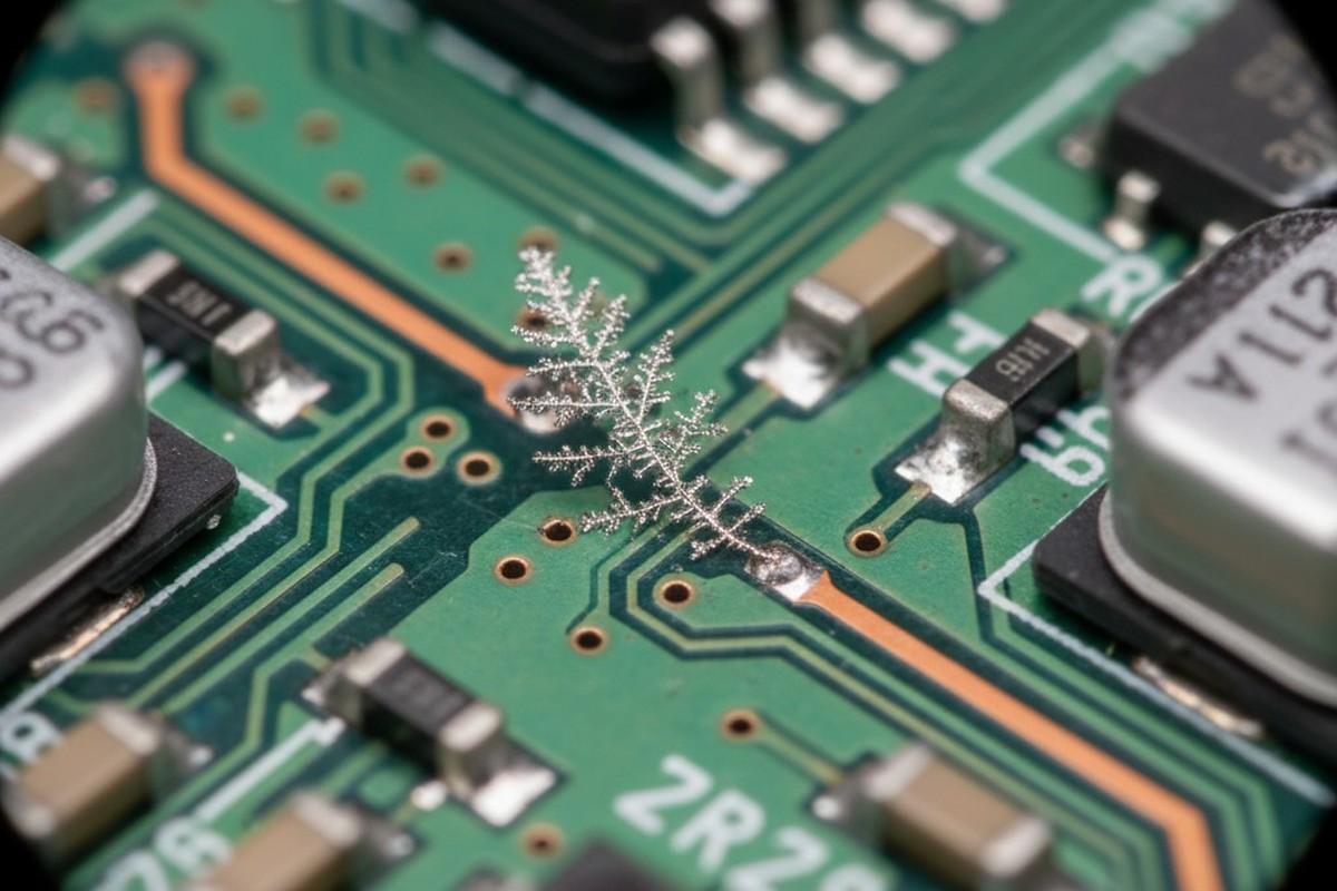
In this “soup,” metal ions from the solder (tin, lead, or silver) dissolve at the anode and migrate toward the cathode. Over time, these ions plate out, building a metallic structure known as a dendrite. It looks like a fern or a tree branch growing across the gap.

This isn’t a fast process. It can take weeks or months. But once that fern bridges the gap, you have a short circuit. At 5V, this might just cause a logic glitch. At 400V, the current rush vaporizes the dendrite, often taking the component and a chunk of the PCB fiberglass with it. The evidence destroys itself, leaving you with a charred board and no clear root cause.
The “No-Clean” Lie at 400V
The industry loves the myth that “No-Clean” flux means you don’t have to clean it. For consumer electronics—your TV remote, a digital toy, a Bluetooth speaker—this is largely true. The voltages are low, and the residue is non-conductive enough to be safe. But when you cross into the industrial and automotive high-voltage domain, “No-Clean” becomes a dangerous misnomer.
At high voltages, the electric field strength is enough to mobilize ions that would be dormant at 12V. Furthermore, “No-Clean” residues are often resin-based, designed to encapsulate the active acids. But heat cycles—like those in an EV inverter—can crack this resin shell. Once the shell cracks, the hygroscopic acid inside is exposed to moisture, and the migration begins.
This is also why you might see conformal coating peeling or blistering. Engineers often blame the coating vendor for adhesion failures. In reality, the coating is semi-permeable to water vapor. Moisture gets through, finds the flux residue underneath, and the resulting outgassing lifts the coating right off the board. You cannot seal in dirt and expect reliability. You are just creating a pressurized failure chamber.
Chemistry, Not Just Washing
So, you decide to clean. This is where most process lines fail. They treat cleaning like doing the dishes—spraying hot water and hoping for the best. But modern flux is not food waste. It is complex chemistry designed to resist water.
Rosin and resin-based fluxes are hydrophobic. Spraying them with Deionized (DI) water is useless; the water just beads up and rolls off, leaving the resin behind. To actually clean a board, you need a chemical reaction called saponification.
We use alkaline saponifiers—specialized chemical agents that react with the fatty acids in the flux vehicle. This reaction turns the insoluble resin into a water-soluble soap. Only then can it be rinsed away. This process requires a precise “wash window.” You need the right concentration of saponifier, matched to the specific flux type you are using, running at the right temperature to drive the reaction.
If the temperature is too low, the reaction is too slow. If the belt speed is too fast, the chemical doesn’t have time to bite. If you use a generic “all-purpose” cleaner without checking compatibility with your solder paste, you might strip the brighteners off your solder joints while leaving the dangerous activators behind. It is a chemical process, not a mechanical scrub.
The Geometry Problem
Even with the right chemistry, you can’t clean what you can’t hit. The trend in modern electronics is toward miniaturization, which creates a nightmare for fluid dynamics.

Take a large QFN (Quad Flat No-lead) component or a heavy IGBT module soldered down to a large copper plane. The standoff height—the gap between the component body and the board—might be less than 50 microns. You have high-voltage rails running right under that component.
Getting a cleaning fluid to penetrate that 50-micron gap against the force of surface tension is incredibly difficult. It requires high impingement pressure and specific spray angles. If your process doesn’t force the saponifier underneath that package, you are creating a “dendrite incubator.” The exposed areas of the board will test clean, but the area under the power FET—the exact place where the voltage is highest and the heat is greatest—remains full of active residue. We often have to force designers to add vias or change component footprints just to make the area washable.
Validation: Proving the Invisible
If visual inspection is useless, what is the metric? How do you know if you actually succeeded?
For decades, the industry used the ROSE test (Resistivity of Solvent Extract). You dunk the board in an alcohol solution and measure how much the resistivity changes. It was fine for 1990s through-hole technology. For modern, high-density, low-standoff designs, the ROSE test is effectively obsolete. It gives you an average cleanliness across the whole board, but it fails to detect the pockets of concentrated evil hiding under a QFN.
The only way to truly validate a high-voltage cleaning process is via SIR (Surface Insulation Resistance) testing. This involves designing a special test coupon with comb patterns that mimic your tightest spacing. You run this coupon through your wash process, then put it in a chamber at 85°C and 85% relative humidity while applying bias voltage. You monitor the resistance for 168 hours or more.
 Testing")
If the resistance drops, you have growth. If it stays high (typically above 100 megohms), your process works. This is the standard set by J-STD-001H. It is rigorous, it is slow, and it is the only way to sleep at night knowing your 800V charger won’t catch fire two years from now.
The Cost of Clean
Implementing a proper inline saponification process with regular SIR validation is not cheap. It requires floor space, chemical management, and waste treatment. But consider the alternative.
In high-voltage systems, reliability is binary. The board is either chemically stable, or it is slowly dying. There is no middle ground. When you are building hardware that handles lethal voltages, the cost of a proper wash process is a rounding error compared to the cost of a recall. Or a lawsuit.


