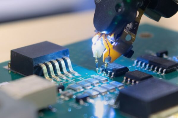
In high-reliability electronics, the most dangerous solder joint isn’t the ugly one. Cold solder joints, bridges, de-wetting—these are obvious defects. Any AOI machine or trained operator will catch them before the board leaves the floor. The true threat to a Class 3 product is the joint that looks perfect. It has a smooth, shiny fillet. It has 100% hole fill. It passes visual inspection with flying colors. But underneath that shiny surface, the copper structure that makes the electrical connection possible has been chemically erased.
Take a common scenario during the transition from prototype to mass production. A facility switches a legacy product to a SAC305 lead-free process. The boards look pristine coming off the selective solder line. Six months later, however, field returns start arriving with intermittent open circuits. Vibration testing shows the leads pulling straight out of the board. A cross-section analysis—the only way to see the truth—reveals the horror: the “knee” of the through-hole barrel is missing. This is the critical junction where the plating bends from the hole wall to the surface pad. It hasn’t cracked. It has dissolved. The solder is holding onto bare fiberglass, and the electrical connection floats on a microscopic layer of brittle intermetallic compound.
This is copper dissolution. It isn’t a mechanical failure; it’s chemical erasure. The solder pot acts as a solvent. In the era of lead-free alloys, ignoring the physics of solubility turns your selective soldering machine into an automated destruction device.
The Physics of a Hungry Alloy
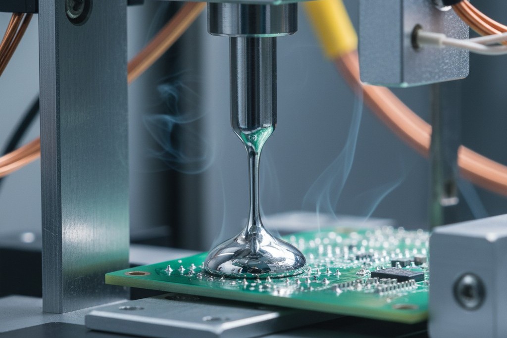
Soldering isn’t gluing; it’s alloying. When molten solder wets a copper surface, it doesn’t just sit on top. It dissolves a portion of the copper to create an intermetallic compound (IMC), usually Cu6Sn5. This layer is necessary for the bond. However, lead-free alloys like SAC305 (Tin-Silver-Copper) are significantly more aggressive solvents than the old Tin-Lead (SnPb) generation. They are hungry for copper.
Two variables drive the rate at which liquid solder eats solid copper: temperature and flow. The Arrhenius equation dictates that for every 10°C rise in pot temperature, the reaction rate (and thus the dissolution rate) accelerates non-linearly. If you run a pot at 290°C or 300°C to force flow into a difficult board, you are accelerating the erosion of the copper plating.
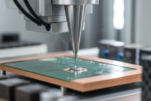
But temperature is only half the equation. Selective soldering adds a dynamic component: flow velocity. Unlike wave soldering, where the board passes over the wave once, a selective nozzle can sit under a pin, pumping fresh, hot, unsaturated solder against the copper surface. This constant replenishment strips away the saturated boundary layer, allowing fresh solder to attack the copper continuously.
A secondary variable often catches maintenance teams off guard: the copper content of the pot itself. As the machine runs, it dissolves copper from the boards, raising the copper percentage in the alloy. This raises the liquidus temperature of the solder, making it “sluggish” or gritty. The natural reaction from a process engineer seeing sluggish solder is to raise the pot temperature. This creates a feedback loop: higher temps dissolve more copper, which raises the melting point, which prompts higher temps. If you aren’t regularly analyzing your solder pot and dumping it when copper levels exceed the alloy manufacturer’s limit (often around 0.9% to 1.0% for SAC305), you are cooking your boards in a bath that requires dangerous temperatures just to flow.
The critical vulnerability in a through-hole joint is the “knee” of the hole. In most PCB fabrication processes, the plating at the knee is thinner than on the flat barrel walls due to the physics of electroplating. If you have 25µm of copper in the barrel, you might only have 15µm or 20µm at the knee. When aggressive selective soldering washes over this area, it attacks from both the top (pad side) and the inside (barrel side). It doesn’t take much dwell time to dissolve 15µm of copper. Once that copper is gone, the solder wets to the epoxy glass of the PCB. It looks connected, but the mechanical integrity is zero.
The Thermal Relief Battleground
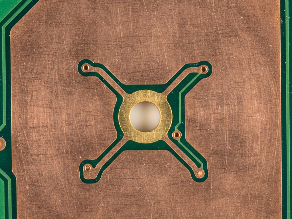
While the physics of dissolution happen in the solder pot, the root cause is almost always found in the CAD data. Poor thermal design on the PCB drives copper dissolution more than any other factor. Specifically, it’s a battle between the electrical requirement for solid ground connections and the manufacturing requirement for thermal relief.
A typical scenario involves a high-current connector pin tied to multiple ground planes on a 12-layer board. If the designer uses a “solid” connection—flooding the copper directly to the pin without thermal relief spokes—that pin becomes a massive heat sink. When the selective solder nozzle touches that pin, the heat instantly wicks away into the inner layers. The solder freezes before it can climb the hole.
The process engineer standing at the machine is now in a bind. The joint won’t fill. They cannot change the board design; the Gerber files are locked. Their only lever is the machine profile. So, they increase the dwell time. Instead of a safe 2-second dwell, they push it to 6, 8, or 10 seconds. They might also bump the pot temperature to 320°C. Eventually, the heat overcomes the thermal mass of the ground planes, and the solder flows to the topside. The joint looks filled. Success? No.
While the heat was struggling to climb the barrel to the topside, the bottom side of the joint—where the nozzle is blasting hot solder—sat in a superheated, high-velocity solvent bath for 10 seconds. The copper at the bottom knee and the lower barrel has been completely stripped away. The operator sees a filled hole and signs off. The cross-section reveals a hollowed-out disaster.
It is vital to distinguish this chemical erosion from mechanical failures like pad lifting. Pad lifting is often a result of thermal shock or mechanical stress where the copper peels away from the fiberglass. Dissolution is different. The copper isn’t peeling; it is vanishing into the solution of the solder pot. If you see “lifted pads” that look ragged or thinned under magnification, you are likely looking at dissolution that weakened the foil to the point of failure.
The Dangerous Logic of “Just a Few More Seconds”
There is no universal “safe” dwell time. Anyone giving you a fixed number like “never exceed 4 seconds” is simplifying to the point of error. A 4-second dwell on a 0.5oz copper board might be fatal, while a 6-second dwell on a 3oz heavy copper backplane might be necessary. However, the non-linearity of the risk is constant. The damage done between second 6 and second 8 is far greater than the damage done between second 1 and second 2.
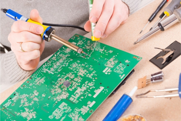
This risk is compounded by rework. In many high-mix manufacturing environments, if a selective solder joint doesn’t fill completely, the board is sent to a hand-soldering station for “touch-up.” This is often the final nail in the coffin. The selective process has already thinned the copper plating significantly. When a technician applies a soldering iron (often set to 750°F/400°C to deal with the heavy ground plane) and adds more flux and wire, they re-initiate the dissolution process on an already compromised barrel.
The irony of the “touch-up” culture is that a hole filled 75% is often mechanically stronger and electrically sufficient (per IPC Class 2 and even some Class 3 conditions) compared to that same hole reworked to achieve 100% fill. The pursuit of visual perfection drives operators to destroy the internal structure of the connection. We essentially burn the house down to paint the roof.
Validation: Trusting Physics Over Eyes
If visual inspection is blind to this failure mode, how do you validate your process? The reality for many organizations is that you cannot validate a selective soldering process for high-reliability products without destructive testing. You must sacrifice boards to save the product line.
This starts with the “Thermal Audit” or process qualification. When profiling a new board, identify the high-mass ground pins. Run the profile that achieves hole fill. Then, take that board and cross-section those specific pins. You need to measure the thickness of the remaining copper at the knee. IPC-6012 Class 3 requires specific remaining plating thickness, but as a general engineering rule, if you see the copper thinning by more than 50% compared to the un-soldered areas, your process is out of control.
If the cross-sections show dissolution, you have three options, none of them easy.
- Introduce bottom-side preheat. By raising the entire board temperature to 110°C-130°C before the nozzle touches it, you reduce the thermal delta the nozzle has to overcome, allowing for shorter dwell times.
- Use a larger nozzle diameter. If clearance allows, a larger flow transfers heat more efficiently than a narrow jet.
- Push back on the design. This is the most difficult but most necessary step. Show the cross-section data to the PCB layout team. A solid ground connection is not “robust” if it forces the manufacturing process to destroy the plating.
Physics does not care about your production schedule or your yield targets. If you combine aggressive lead-free alloys, high temperatures, and long dwell times, the copper will dissolve. The only defense is to stop looking at the shiny fillet on top and start worrying about the invisible erosion underneath.

