The Invisible Failure
The most dangerous board in a high-reliability assembly isn’t the one that fails functional test. It’s the one that passes. You can hold a board up to the light, see a perfect top-side fillet, and sign off on the lot, but if that joint is destined for an aerospace cockpit or a medical device, visual inspection is effectively a lie.
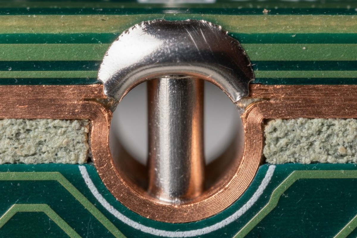
Physics dictates that a perfect fillet on the top pad does not guarantee a solid column of solder inside the barrel. In Class 3 manufacturing, where J-STD-001 demands 75% vertical fill (and often 100% depending on contract addendums), the “good enough” visual check is a liability. You can have a beautiful meniscus on the component side while the barrel itself is riddled with voids or filled only halfway.
The only impartial judge here is X-ray analysis or destructive cross-sectioning. When you cut that sample board and polish the cross-section, you aren’t looking for craftsmanship; you are looking for evidence of a fight between capillary action and thermal dynamics. When solder fails to climb, it rarely means the wave height was too low. It usually means the board design physically made ascent impossible.
The Geometry of Gas Lock
The primary culprit for poor vertical fill is almost always the hole-to-lead ratio. Designers and procurement teams often treat component pins and plated through-holes (PTH) as simple “tab A into slot B” geometry. If the pin fits, the design is approved. But in wave soldering, the hole is not just a receptacle; it is a fluid dynamic channel.
Watch what happens when procurement swaps a round pin for a square one to save a fraction of a cent. The diagonal of that square pin might technically clear the hole wall, but the corners create tight pockets where flux gas gets trapped. As the wave hits the bottom of the board, the flux activates and outgasses. If there is no annulus—no clear “chimney” of air space around the pin—that gas has nowhere to go. It forms a pressurized bubble inside the barrel.
You are trying to push liquid solder up against a high-pressure gas pocket. Physics wins every time. The solder stops, the gas stays, and you get a blow-hole or a void.

This issue is even more aggressive with Pin-in-Paste (PIP) processes. The paste volume adds another variable to the gas equation, but the fundamental rule remains: gas must escape for solder to enter.
To achieve Class 3 fill, you need a specific clearance annulus. The IPC recommends ranges, but experience dictates that for a standard 0.062″ to 0.093″ thick board, you need a clearance of roughly 0.010 inches (10 mils) over the pin diameter. If you are working with a 0.028″ pin and a 0.032″ finished hole, you have 4 mils of clearance—2 mils on either side if perfectly centered. That is like trying to drink a milkshake through a coffee stirrer. The capillary pressure required to overcome the drag and the back-pressure of the flux gas is simply too high. The solder will bridge on the bottom before it ever reaches the top.
The Thermal Heist
Even if the geometry allows for flow, the board itself often acts as an enemy combatant. We tend to treat the PCB as a passive carrier, but thermally, a multi-layer board is a massive heat sink.
Take a 14-layer server backplane with heavy ground planes on layers 4 through 10. When that board hits the wave, the solder is at 260°C (for SAC305), but the copper barrel is cold. The moment liquid solder touches the barrel wall, the internal ground planes suck that thermal energy away instantly. The solder freezes against the wall before it can climb. It doesn’t matter how high you pump the wave; you cannot pump liquid through a frozen plug.
This is where the debate about “selective soldering” often arises. Engineers assume selective soldering fixes this because it’s more precise, but selective pots have significantly less thermal mass than a full wave tunnel. If you can’t fill it on a wave, you will struggle even more on a selective machine without aggressive pre-heating.

You won’t solve this with pot temperature. The real fix lies in the pre-heat soak. You must saturate the core of the board. The goal is to get the “knee” of the hole—the internal copper structure—up to at least 110°C or 120°C before it ever touches the wave. You are minimizing the “Delta T” (the temperature difference) between the solder and the copper. If the board is hot enough, the solder stays liquid long enough to climb the tower. If you rely on the wave to heat the barrel, you have already lost.
You Cannot Fix Design with Wave Height
A common reaction on the floor when fill rates drop is to “crank the parameters.” Operators increase the pump RPM to raise the wave height or slow the conveyor to a crawl to increase dwell time. This is effectively trying to brute-force physics.
Raising the wave height increases the hydrostatic pressure, yes, but it mostly just increases the risk of bridging and shorts on the bottom side. Increasing the dwell time—letting the board sit in the wave longer—is even more dangerous. If you dwell too long, you risk leaching the copper right off the knee of the hole or dissolving the annular ring. You might get the fill, but you’ve destroyed the metallurgical integrity of the via.
Top-side “touch-up” or hand-soldering is just as dangerous for Class 3 failures. Adding wire solder from the top creates a “cold joint” interface where the new solder meets the old solder inside the barrel. It looks filled, but structurally, it’s a weak point that will fracture under vibration.
The Drill Chart is the Process Window
There is no magical flux and no perfect machine setting that compensates for a 24-layer board with 3-mil clearance holes and insufficient thermal relief. We are skipping the basics of machine maintenance here—assuming your nozzle is clean and your impeller is working—because no amount of maintenance fixes a bad drill chart.
If you want Class 3 fill, the work happens in the CAD software long before the board hits the wave solder pot. You must design the hole to breathe (ratio) and the board to hold heat (thermal relief). If the design doesn’t account for fluid dynamics and thermodynamics, the only thing you will be manufacturing is scrap.


