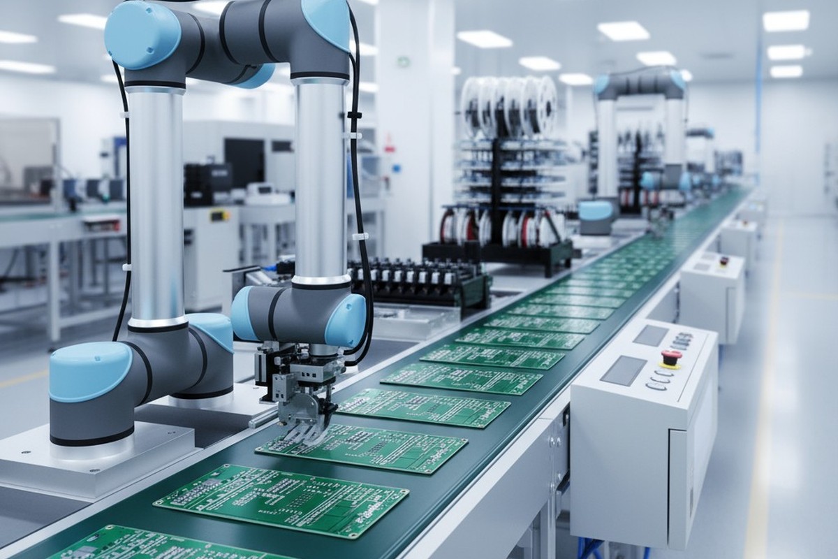
The sound is unmistakable. A sharp crack, followed by the sinking feeling that another board is heading for the scrap pile. It tore right at the curve, taking a sliver of solder mask with it and leaving a jagged edge that will never fit its enclosure. This is the cost of treating PCB panelization as an afterthought—a final checkbox before production. For simple rectangular boards, the cheapest method might suffice. But for designs with irregular contours, tight tolerances, or brittle substrates, your panelization strategy is not a cost-saving measure. It is a critical defense for your product’s quality and your project’s budget.

At Bester PCBA, we’ve seen countless designs where a few cents saved on panelization led to thousands of dollars lost in scrap, rework, and delays. The default method of using mouse-bites is a blunt instrument in a process that demands surgical precision. Choosing the right depaneling method is a fundamental Design for Manufacturability decision that protects your investment and requires moving beyond the simple snap to a more engineered approach.
The Hidden Liability of Mouse-Bites: When the Cheap Route Costs You More
Mouse-bites, the small clusters of holes drilled along a board’s perimeter, are the industry’s default for a reason: they are cheap and fast. They create a line of weakness, allowing an operator to snap boards from the panel with brute force. For a straight-edged, robust FR-4 board, this works well enough. The trouble begins when this logic is applied to boards that are anything but simple.
The Physics of Failure: Stress Concentration on Curved Edges
Think of tearing a perforated sheet of paper. The force travels neatly along the dotted line because the stress is distributed evenly along a straight path. An irregular or curved outline shatters this principle. When you apply bending force to a curve, stress no longer follows the intended path of the mouse-bites. Instead, it concentrates at the sharpest points of the curve or the corners of the breakaway holes. This localized stress exceeds the material’s strength, causing a fracture that veers off-path and tears into the board, leaving a jagged, uncontrolled break.
Brittle Materials and Micro-Cracks: Why Ceramics and Rogers Can’t Handle the Snap
This problem is amplified when working with brittle substrates. Materials like ceramics, Rogers, or even very thin FR-4 lack the ductility of standard fiberglass; they cannot bend to absorb the stress of being snapped. When subjected to the sharp, localized force from a mouse-bite separation, they don’t tear—they shatter. This can manifest as a catastrophic crack across the board or, more insidiously, as microscopic fractures in the substrate or the solder joints of nearby components. Solder mask, a thin and brittle coating, is often the first casualty, flaking away from the edge and compromising the board’s long-term reliability. For these materials, using mouse-bites isn’t a calculated risk; it’s a guarantee of future failure.
The Pragmatic Solution: Designing with Routed Tabs and Stress Relief
When the risk of uncontrolled fracture is unacceptable, you must abandon the “breaking” mindset entirely. The more robust approach is to use routed breakout tabs. This method involves routing the board’s full profile, leaving it attached to the panel frame by a few small, well-placed tabs of material.
Tab vs. Mouse-Bite: From Breaking to Controlled Separation

The conceptual difference is critical. With mouse-bites, the entire board edge is a weakened perforation designed to be broken. With routed tabs, the board edge is a perfectly finished, smooth contour. The tabs are not lines of weakness but small structural supports that hold the board during assembly. Depaneling is no longer an act of snapping but one of controlled cutting or breaking at a few specific, engineered locations. This gives the designer total control over where separation force is applied, protecting the rest of the board from mechanical stress.
Essential Design Rules for Robust Breakout Tabs
Simply using tabs isn’t enough; they must be designed correctly. At Bester PCBA, we find the most reliable designs follow a few core principles.
Tab Placement and Distribution: Distribute tabs as evenly as possible around the board’s perimeter for stable support during assembly. Avoid grouping them on one side. For odd shapes, place tabs at extremities to prevent sagging or vibration during pick-and-place. Tab width is a trade-off; we recommend 2 mm to 5 mm. Too narrow, and the board may be insecure; too wide, and it requires excessive force to remove.
Perf-Tabs for Cleaner Breaks: For the cleanest separation, we advocate for “perf-tabs” or “stamp-hole” tabs. This involves drilling a series of small, non-plated holes (typically 0.5 mm to 0.8 mm) across the base of the tab. These perforations function like localized mouse-bites, ensuring that when the tab is broken, the fracture occurs cleanly at the board edge. This leaves a much smaller and smoother remnant than a solid tab and must be clearly specified in your fabrication drawings.
When Precision is Non-Negotiable: The Case for Laser Depaneling
For the most demanding applications, even the minor remnant from a well-designed perf-tab is too much. When edge smoothness is a critical mechanical requirement, when boards are dense with sensitive components, or when the substrate is exceptionally fragile, the ultimate solution is laser depaneling.
Zero Stress, Perfect Edges: How Laser Cutting Liberates Your Design

Laser depaneling is a non-contact process. It uses a high-power focused laser beam to ablate, or vaporize, the substrate material along the board outline. Because nothing physically touches the board, the process is entirely free of mechanical stress—no bending, no torque, and no shock transferred to components or their solder joints. The laser can follow any contour with micron-level precision, producing a perfectly smooth, sealed edge with no burrs or fractures. This liberates the designer, allowing components to be placed much closer to the board edge than any mechanical method would permit.
Making the Call: Routed Tabs vs. Laser Depaneling
The choice between routed tabs and laser depaneling comes down to your project’s specific needs. While routed tabs are a significant improvement over mouse-bites, laser cutting offers unmatched quality and precision. We use the following framework to guide our clients.
| Feature | Routed Tabs (with Perf-Holes) | Laser Depaneling |
|---|---|---|
| Mechanical Stress | Low | Zero |
| Edge Quality | Good, with small remnant | Perfect, smooth |
| Feature Proximity | Good (~3mm from edge) | Excellent (~0.5mm from edge) |
| Initial Cost | Moderate | High |
| Material Support | Excellent for most materials | Best for brittle & flex |
Enforcing Success: Critical DFM Rules for Tab-Routed Panels
Choosing the right method is only half the battle. To ensure high yields, that choice must be supported by rigorous design rules. A great panelization strategy can be undone by a single misplaced component, and this is where manufacturing expertise is paramount.
The Sanctity of the Keepout: Protecting Components and Traces

We consider the area around a breakout tab sacred ground. When a tab is broken, it flexes. Even minor flexion can transfer stress to the surrounding board, cracking the solder joints of a nearby capacitor or fracturing a delicate BGA. For this reason, keepouts around tabs are not a suggestion; they are a requirement. We enforce a strict keepout zone, typically extending 3-5 mm from the tab into the board, where no components or critical traces are allowed. Ignoring this rule is an invitation for intermittent faults and field failures.
Scrap will do the enforcing.
Rethinking Fiducials: Achieving Alignment on Odd-Shaped Arrays
Standard panel design uses three fiducial markers on the panel frame for global alignment, assuming a uniform, repeating pattern. Irregularly shaped PCBs are often nested in non-uniform arrays to maximize panel usage. Here, global fiducials are not enough to guarantee precise alignment for every board. The solution is to use local fiducials. Placing two or three small fiducials near each board or cluster allows the assembly machine to correct for minor rotation or positional errors within the panel. This is critical for fine-pitch components and a prerequisite for laser depaneling.
The Bester PCBA Stance: A Yield-First Approach to Panelization
The conversation around panelization is too often dominated by upfront cost—a flawed perspective. The true cost of a panelization strategy isn’t measured on the fabrication quote, but in the final yield of good, reliable boards. A cheap method that produces 10% scrap is vastly more expensive than a robust method that produces none.
At Bester PCBA, our guidance is unambiguous. We advocate for the panelization method that best protects the integrity of your design. For irregular contours and brittle materials, this means leaving mouse-bites behind and embracing the engineered control of routed tabs or the absolute precision of laser cutting. This isn’t about upselling a service; it’s about protecting your product.
It’s about manufacturing with intent.


 PCB Technology: Types, Benefits, Challenges, and Applications")