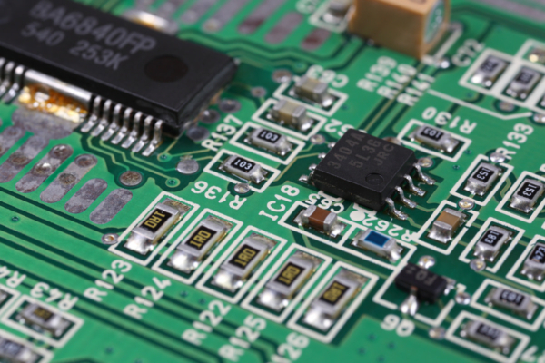
An engineer looking to modernize a legacy circuit board often sees a clear path forward. By retrofitting a classic through-hole (THT) design with modern surface-mount (SMT) components, a product can gain new functionality and shrink in size. In the clean, two-dimensional world of a CAD layout, this combination appears straightforward. But on the factory floor, where designs become physical objects, this simple upgrade initiates a profound manufacturing conflict.
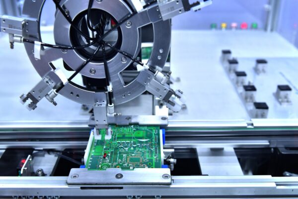
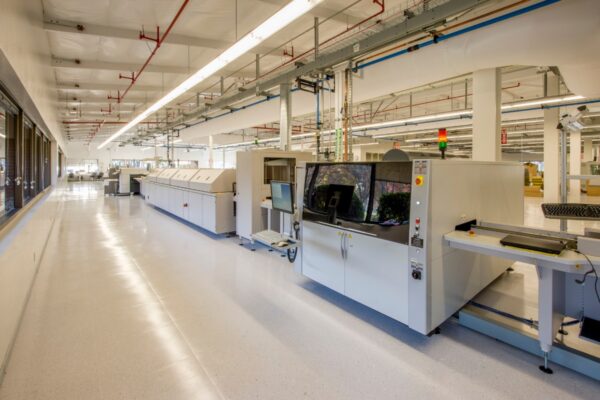
A board designed exclusively for through-hole components anticipates a simple, almost rustic process. Components are inserted, and the board is sent through a wave of molten solder. The introduction of SMT, however, is not an addition but a transformation of the entire manufacturing reality. It demands cleanrooms, solder paste printers, and robotic pick-and-place machines. More critically, it forces the board through a reflow oven, a full-board heating cycle that the original PCB substrate and its stalwart THT components were never meant to withstand. This single change introduces stresses that can warp the board, cause its layers to delaminate, and turn trapped moisture into a destructive force. The design choice creates a cascade of risk that must be managed from the moment the first SMT pad is placed.
The Core Challenge: A Tale of Two Thermal Worlds
At the heart of every mixed-technology assembly lies a fundamental clash of thermal philosophies. Each component type was conceived for a radically different soldering environment, and forcing them to coexist on a single board creates an inherent tension that is the root cause of most manufacturing defects.
Surface-mount components expect the controlled, gentle environment of a reflow oven. The entire assembly is carefully preheated, brought to a peak temperature around 245°C just long enough to melt the solder paste, and then cooled with equal precision. The process treats the board as a single, unified thermal mass. It is a process defined by uniformity and control.
Through-hole components, by contrast, were born from a process of localized, aggressive heat. In wave soldering, only the bottom of the board is dragged across a flowing wave of solder, often at a much hotter 260°C. The heating is rapid and intense, confined to the solder side. When you force these two worlds together, you are left with no ideal options. You must either subject the board to multiple, stressful heating cycles, or you must attempt a single process that pushes one set of components far beyond its intended limits.
Navigating the Compromise: Choosing an Assembly Sequence
To resolve this thermal conflict, manufacturers have developed three primary pathways. The choice is not merely technical; it is a strategic decision with deep consequences for cost, production speed, and the ultimate reliability of the board.
The oldest method involves placing and reflowing SMT components first, then inserting the THT parts and running the entire board through a wave soldering machine. For high-volume production, this sequence is fast and economical. But it comes with a heavy price in risk. Any SMT components on the bottom of the board must be glued down, and they must be robust enough to survive a violent immersion in a 260°C solder wave. It is a brutal test that many components are not designed to pass.
A more modern and far more gentle approach also begins with the standard SMT reflow process. Afterward, however, a selective soldering robot addresses the THT components. A small, programmable fountain of solder is dispensed by a nozzle that targets only the individual THT pins. This keeps the intense heat localized, protecting the rest of the board. The process is significantly safer for sensitive components, but that safety comes at a cost. The robotic systems are a major capital expense, and because the process is serial, soldering one joint at a time, it is inherently slower than wave soldering.
The third path seeks the ultimate efficiency of a single-process reflow. Using a technique known as Pin-in-Paste (PiP), high-temperature-rated THT components are inserted into holes that have been printed with solder paste, just like SMT pads. The entire board, with both component types in place, then goes through the reflow oven once. This eliminates an entire soldering step, but its success depends on a level of process control that leaves little room for error.
The Precision Problem of Pin-in-Paste
The viability of the Pin-in-Paste process rests entirely on a single, difficult variable: solder paste volume. The amount of paste printed into the through-hole must be calculated with extreme precision. It needs to be just enough to fill the gap between the component lead and the plated barrel of the hole, a requirement known as “barrel fill,” while also forming proper solder fillets on both sides of the board.
This creates an exceptionally narrow process window. Too little paste results in a weak joint with insufficient fill, a defect that violates industry standards like IPC-A-610, which often requires over 75% vertical fill. Yet, too much paste gets squeezed out when the component is inserted. These excess deposits can become solder balls that migrate during reflow, creating disastrous short circuits. Achieving the correct volume demands custom-designed stencils and a printing process with near-perfect repeatability, making it a far more sensitive operation than standard SMT assembly.
When “Good Enough” Isn’t: Preforms vs. Pin-in-Paste
For applications where the integrity of a THT joint is non-negotiable, such as with high-thermal-mass connectors in aerospace or medical devices, the process risk of Pin-in-Paste can be unacceptable. Here, manufacturers face a classic trade-off between process cost and guaranteed reliability, weighing PiP against an alternative: solder preforms.
Preforms are small, precisely engineered shapes of solder alloy placed in or around the through-holes before component insertion. They are a material solution, not a process one. They guarantee a specific, repeatable volume of solder for every single joint, resulting in exceptionally robust connections. The trade-off is cost and complexity. Preforms are an additional component to be sourced, managed, and placed on the board, adding both material expense and another process step. The decision becomes strategic. Pin-in-Paste is a clever solution for cost-sensitive products where its process variability is an acceptable risk. Solder preforms are an insurance policy for high-reliability applications where a joint failure is not an option.
The 3D Reality of the Factory Floor
In the abstract space of a layout tool, a circuit board is a two-dimensional plane. This perspective is the source of the single most frequent and costly mistake designers make when creating a mixed-technology board. They forget that soldering equipment is three-dimensional machinery that needs physical space to operate.
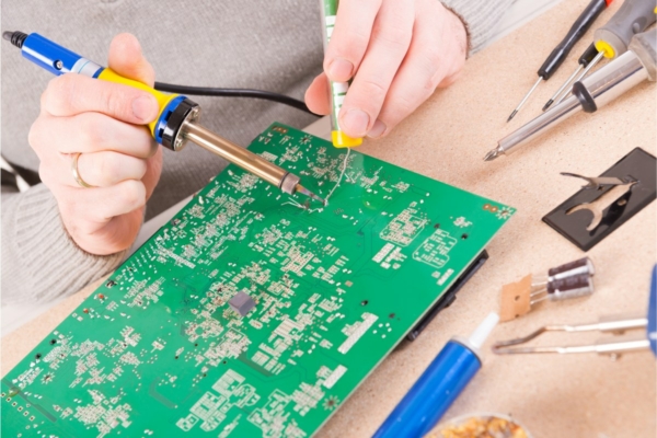
During wave soldering, a tall THT component can cast a “solder shadow,” a wake that physically blocks the flow of molten solder from reaching smaller SMT components downstream. Depending on the component’s height, this can require a keep-out zone of 15mm or more. For selective soldering, the robotic nozzle needs a clear radius of 3 to 5mm around each pin to approach, solder, and retract without crashing into an adjacent part. Placing a tall capacitor or connector inside this zone makes automated soldering impossible. This simple oversight, born from a 2D mindset, forces the assembly to be finished by hand—a slow, expensive, and far less repeatable process that erodes profit and introduces quality risks.
Anatomy of a Failure
When the thermal conflicts and physical realities of mixed-technology assembly are ignored during design, a unique class of defects emerges. These are not the typical problems of any assembly process; they are the direct, predictable consequences of forcing two incompatible technologies together.
The solder shadowing created by a tall THT component in a wave process leaves SMT pads downstream completely untouched by solder, resulting in an open circuit. Elsewhere on the board, the thermal shock of that same 260°C wave can be catastrophic for bottom-side SMT parts. It is known to cause microscopic cracks in ceramic capacitors and inflict latent damage on sensitive integrated circuits, leading to mysterious field failures months after the product has shipped.
Even the equipment meant to protect the board can become a source of failure. The composite material used for wave solder pallets is an excellent thermal insulator. While it effectively shields SMT components, it also blocks the infrared pre-heaters. If a process engineer fails to develop a custom thermal profile that accounts for this, the board arrives at the solder wave without being sufficiently preheated. The resulting thermal shock leads to poor solder flow and the very defect the process was trying to avoid: insufficient hole fill in the THT components. Over time, the accumulated stress from these multiple, harsh heating cycles can cause the entire board to warp, breaking the delicate connections of large components like BGAs and creating intermittent failures that are nearly impossible to diagnose.
Designing for Manufacture: A Shift in Perspective
The most effective solutions to these challenges are not found in more advanced machinery or complex inspection. They are found in the initial design phase, by adopting a mindset that anticipates the manufacturing process from the very beginning.
Protecting the Vulnerable
The core strategy is to shield sensitive and expensive SMT components from the unavoidable harshness of the THT soldering process. This begins with the layout. The most reliable practice is to place all high-value parts—processors, BGAs, and fine-pitch ICs—on the top side of the board. With THT components also inserted from the top, all the aggressive soldering action, whether wave or selective, is confined to the bottom side, far from anything vulnerable.
Beyond placement, the designer holds the power to specify the process. Requesting selective soldering in the manufacturing notes is the surest way to protect the assembly. If high volume or cost pressure makes wave soldering a necessity, the solution is to collaborate with the manufacturer on a custom wave pallet. This fixture is meticulously designed with pockets and shields that act as a thermal barrier, physically covering the SMT components on the bottom side as they pass over the molten wave. It is a solution born from experience, acknowledging the physical reality of the factory floor and designing for it, rather than in spite of it.
