What is Embedded Traces
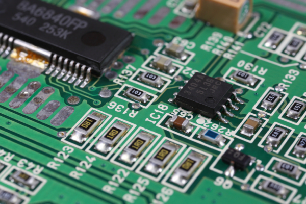
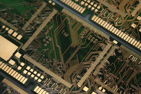
Embedded traces are conductive pathways or tracks that are integrated within the layers of a printed circuit board. These traces are specifically designed to carry electrical signals or power between the embedded components. They are typically made of copper and are etched onto the inner layers of the PCB during the manufacturing process.
The embedding traces within the PCB layers optimize space utilization and improve the overall performance of the circuit. By integrating the traces, PCB manufacturers can accommodate more components and reduce the surface area required for surface-mounted components. This is particularly important for smaller devices that have limited surface mounting areas.
Embedded traces also offer several advantages in terms of reducing electromagnetic interference (EMI) and improving signal integrity. By integrating the traces within the PCB layers, the electromagnetic radiation emitted by the circuit is minimized, resulting in reduced interference with other nearby electronic devices. Additionally, embedding the traces helps to reduce inductive reactance, improving the overall electrical performance of the circuit.
Various techniques, such as blind vias, buried vias, and microvias, are employed to establish connections between the embedded components and the outer layers of the PCB. These techniques ensure proper connectivity while maintaining the integrity of the embedded traces.
