What is Hole Location
Hole location is the strategic placement of non-plated-through holes (NPTH) on a printed circuit board for accurate positioning and alignment during manufacturing processes. These holes, also known as tooling holes or locating holes, are strategically placed based on the machine’s requirements.
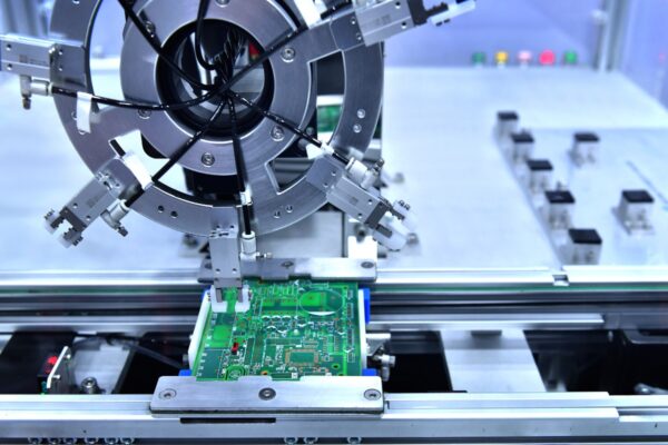
Hole Location aims to ensure precise alignment of the PCB during various manufacturing processes. Using custom-fit holding pins can keep the tolerance for further processing very low, resulting in accurate and consistent results. Hole Location is particularly useful in stack processing, where multiple PCBs are processed simultaneously. The hole locations serve as reference points for aligning the stack, ensuring that drilling or milling operations are performed accurately on each individual board within the stack.
Hole Location differs from plated-through holes (PTH), which are used for electrical connections between different layers of the PCB. Hole Location, on the other hand, is not intended for electrical connections but rather for precise positioning and alignment purposes.

