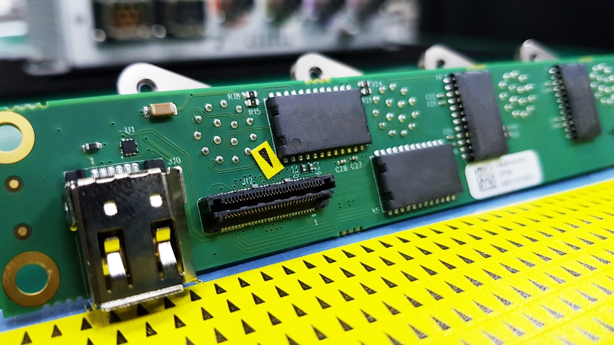
PCB assembly is the process of installing electronic components such as resistors, transistors, and diodes onto a printed circuit board. It can be done manually or mechanically.
PCB assembly and PCB manufacturing involve completely different processes:
- PCB manufacturing includes a wide range of processes, including design and prototype design.
- PCB assembly only starts after the PCB manufacturing process is completed, focusing on component placement.
We will dive into various PCB assembly technologies, the specific processes involved, and suggestions on how to assemble PCBs more effectively.
Pcb Assembly Technology
PCB assembly technologies have evolved significantly with the progress of electronic technologies. Currently, there are three commonly used assembly technologies.
Surface Mount Technology(SMT)
SMT assembly solders surface-mounted devices (SMD) onto PCBs. Due to the small packaging used for SMD components, the entire process must be carefully controlled to ensure the accuracy of solder joints and appropriate temperature. Fortunately, SMT is a fully automated assembly technology. It uses machines to pick up individual components and place them on a PCB with extremely high accuracy.
The whole SMT process usually includes the following steps:
- Steel screen printing
- Solder paste printing
- Component mounting
- SPI
- Reflow soldering
- AOI
- Plate cleaning
- Plate splitting
- Test assembly
Thru-Hole Technology(THT)
Thru-hole technology is a more traditional PCB assembly method. It inserts electronic components such as capacitors, coils, large resistors, and inductors into the circuit board through pre-drilled holes. Unlike SMT, THT can assemble larger and heavier electronic components and provide stronger mechanical bonding, making it more suitable for testing and prototype design purposes.
Mixed PCB Assembly Technology
As electronic products become smaller and more complex, the demand for PCB assembly is increasing. It can be challenging to assemble highly complex circuits in limited space only using SMT or THT technology separately. Therefore, the combination of SMT and THT is often necessary. When using hybrid PCB assembly technology, appropriate adjustments must be made to simplify the welding and assembly process.
PCB Assembly(PCBA) Process
Step 1: Bare Board Baking
Bare PCB baking to ensure dryness of PCB board.
Step 2: Solder Paste Printing
To apply solder paste in PCB assembly, first print solder paste onto the areas where components will be placed with a stainless steel stencil. A mechanical fixture holds the stencil and the PCB together, and an applicator is used to print the solder paste evenly to all the openings in the board. Once the applicator is removed, the paste will remain only in the desired areas of the PCB. The solder paste used in this process is grey in color and is made up of 96.5% tin, 3% silver, and 0.5% copper, making it lead-free.
Step 3: High-Speed SMT Mounting
The Pick and Place machine can accurately connect components to the PCB by using a robotic arm to pick them up and place them on the PCB according to a predetermined design. The machine “draws” the components onto the PCB by placing them in the correct position on the solder paste. This process ensures the accurate placement of components, which is crucial for the overall functionality and reliability of PCB components.
Step 4: Reflow Soldering
Reflow soldering is a process commonly used in electronic manufacturing connecting electronic components to printed circuit boards(PCB). During this process, solder paste is applied to the PCB where the component will be installed, and then the component is placed on the solder paste. Then, the PCB with the components connected is heated to a temperature sufficient to melt the solder paste through a reflux furnace, and a solid and permanent connection is established between the components and the circuit board. The temperature used for reflow soldering may vary depending on the type of solder and component used, usually around 250 °C.
Step 5: AOI
After completing the soldering of the printed circuit board, it comes to use AOI instruments to detect the soldering condition of the PCB. AOI, or automatic optical inspection, is a common method used in electronic manufacturing to check for defects in printed circuit boards after the soldering process. AOI can detect missing components, incorrect component placement, and solder joint defects such as bridges, open circuits, and insufficient solder. By automating the detection process, AOI can greatly improve detection efficiency and accuracy and help ensure the quality of the final product.
Step 6: Wave Soldering
Wave soldering is a widely used method for soldering through-hole components on printed circuit boards. In this process, the PCB is first assembled with through-hole components and then melted with a wave of solder in a special oven called a wave soldering machine. The melted solder waves wet and solder the exposed leads of the components to the corresponding copper solder pads on the bottom side of the PCB.
However, wave soldering can also be used for double-sided PCBs, and additional precautions are taken to prevent damage to the opposite component. This can include masking the opposite side with protective materials or pre-welding the opposite side before wave soldering to provide additional support and prevent component movement during the process.
After the wave soldering process, PCBs are usually sent for cleaning and inspection to remove any excess flux or solder and to check whether there are any welding defects or other problems that may affect the performance of the final product.
Step 7: Cleaning
After wave soldering, the PCB should be cleaned to remove any excess flux or solder residue that may remain on the board. This is crucial for ensuring that the final product is defect free and functioning properly.
After the cleaning process is completed, the circuit board should be inspected to ensure that there are no pollutants or defects that may affect its performance.
Step 8: Quality Checking
Now it comes to functional testing, which is a key step in the PCBA process, involving verifying the functionality and electrical characteristics of the PCB. At this stage, the PCB is tested to ensure compliance with design specifications and requirements.
Function tests can include applying input signal and power supply to PCB and measuring the output signal of each point on board with oscilloscopes, digital multimeters, function generators and other instruments. Testing can also include checking the operation of individual components on a PCB and verifying whether they operate as expected.
If any parameters tested do not meet the specifications, the PCB may be rejected and scrapped or reworked according to the company’s standard procedures. The functional testing phase is a key step in ensuring that the final product has high quality and meets design requirements.
Step 9: Final Cleaning, Packing, and Shipment
Once the functional testing phase is complete and the PCB has been verified to meet the requirements and specifications of the design, it is time to clean the unwanted residual flux, finger dirt, and oil stains.
The final cleaning phase typically involves using a specialized cleaning solution or deionized water to remove any residual flux, finger dirt, or oil stains that may be left behind on the surface of the board. A high-pressure washing tool may be used to clean the board thoroughly without damaging the PCB circuit. After washing, the board is typically dried using compressed air to ensure that there is no residual moisture left on the board.
Once the final cleaning and drying process is complete, the PCB is ready for packaging and shipment. The PCB may be packed in anti-static bags or specialized packaging material to protect it during shipping and ensure that it arrives at its destination in good condition. The packaging may also include labeling or other documentation to identify the PCB and provide information about its specifications and requirements.
Pay Special Attention to File Formats
The file format used for PCB design and manufacturing is an important consideration in this process. The file format used is usually standard ASCII text format, which can create the physical layout of printed circuit boards. The file format must be compatible with the software used by PCB manufacturers to ensure the accurate conversion of designs into physical PCBs.
It is also important to consider naming and labeling parts when creating designs. Each component on the printed circuit board should be clearly marked and identified to avoid errors during assembly and testing. Labels should also be consistent and standardized to ensure that the design is easy to understand and follow.
In addition to labeling, it is also necessary to consider trade-offs when designing a PCB. Balancing involves choosing between different design considerations, such as power, transmission, and size. It is important to balance these trade-offs to achieve the required performance and functionality while ensuring that the design can be effectively manufactured and assembled.
If necessary, it is recommended to consult the manufacturer to understand the techniques for improving the design and meeting the requirements. Collaboration between designers and manufacturers can lead to more efficient PCB design and manufacturing processes.
PCB Assembly Service at Bester
It is always reassuring to collaborate with PCBA providers with a good record in quality and reliability. Bester Technology has passed ISO9001, IPC, and UL certifications, demonstrating its commitment to meeting high industry standards.
Bester has experienced engineers that can provide advice and work closely with clients. This helps to ensure that the feasibility of the assembly project is fully considered and any potential issues are addressed early in the process. It is also important to have a supplier who can handle various assembly requirements from prototypes to mass production.
For many customers who need to quick-delivered PCBA to keep up with their production schedules, a short turnaround time is crucial. Bester stores a large inventory of common parts, which is also an advantage. This helps to minimize delays and ensure that production schedules are met. Bester can always provide excellent PCBA in a short TAT.
In situations where specific components cannot be purchased, Best Technology engineers can provide recommendations for affordable alternatives, which is reassuring. This helps to control costs while ensuring that PCBA meets the required specifications. Our component procurement method is a powerful asset that demonstrates its commitment to meeting customer needs in a timely, cost-effective manner.
Overall, these factors make Bester Technology a strong choice for customers seeking reliable and high-quality PCBA providers.


 Circuit Board Assembly")

