PCB fabrication is the process of creating bare boards that will serve as the foundation for printed circuit board assembly. It is essential to choose your PCB fabrication contractor carefully, as even small errors can render the entire board useless. Effective communication between the design team and manufacturers is critical, especially as manufacturing has increasingly moved overseas.
In this post, we will delve into everything you need to know about the PCB fabrication process. We will cover the pre-process, the full PCB fabrication process, and important considerations to keep in mind when selecting a PCB fabrication company.
What Is PCB Fabrication
PCB fabrication is the process of transforming a circuit board design into a physical structure based on the specifications provided in the PCB design package. It involves a series of steps and techniques to produce a functional PCB.
PCB fabrication is a crucial step in the PCB development process. It translates the design into a physical board that can be assembled with electronic components to create a functional electronic device. The quality of the fabrication process directly impacts the reliability of the PCB. It ensures that the PCB meets the required specifications and provides optimal electrical performance, signal transmission, and durability.
PCB fabrication is just one part of the overall PCB manufacturing process. PCB assembly is a separate step that follows PCB fabrication, which involves placing components onto the board to make it functional. While PCB fabrication focuses on creating the physical structure of the board.
What is the Difference Between PCB Fabrication and PCB Assembly Process
PCB fabrication and PCB assembly are two crucial steps in the PCB manufacturing process.
PCB Fabrication
PCB fabrication involves translating a circuit board design into a physical board structure. It’s like creating the blueprint for a city, with paths, streets, and zoning. In this process, the design is transferred onto the board using various techniques such as etching or printing. The goal is to create a robust and reliable foundation for the electronic components to be placed on.
PCB Assembly
PCB assembly is the process of actually placing components onto the fabricated board to make it functional. It’s like constructing buildings in a city. During this process, electronic components such as resistors, capacitors, and microchips are soldered onto the board. These components work together to create the desired electronic circuit. PCB assembly brings the board to life and allows it to perform its intended function.
PCB assembly is a delicate process that requires precision and expertise. The components must be placed accurately and soldered properly to ensure a reliable and high-performance PCB.
The Difference
PCB fabrication focuses on creating the physical structure of the board, while PCB assembly involves adding the electronic components to make the board operational. Both processes are essential and go hand in hand to create a functional and reliable printed circuit board.
Before the PCB Fabrication Process
Fabricating a printed circuit board requires careful attention to detail. Before you begin the process, it is essential to complete several important steps to ensure a successful board build. Let’s take a closer look at these steps:
Conduct a Comprehensive Engineering Review for Circuitry
Before starting the PCB fabrication process, it is crucial to conduct a thorough engineering review of the circuitry. This review involves carefully examining the design to identify any potential issues or areas for improvement. By conducting this review, you can catch any errors or inconsistencies early on, saving time and resources in the long run.
Synchronize Schematic and Layout Databases
To avoid any discrepancies or misalignments, it is vital to synchronize the schematic and layout databases. This step ensures that the design is accurately represented in both the schematic and the physical layout of the PCB. By synchronizing these databases, you can prevent any inconsistencies that may arise during the fabrication process.
Perform Complete Circuit Simulation, Signal Integrity, and Power Integrity Analysis
To ensure the functionality and reliability of the PCB, it is essential to perform comprehensive circuit simulation, signal integrity, and power integrity analysis. These analyses help identify any potential issues with the circuit design, such as signal interference or power distribution problems. By addressing these issues before fabrication, you can avoid costly rework or troubleshooting later on.
Verify PCB Design Rules and Constraints
Before proceeding with the fabrication process, it is critical to verify that the PCB design adheres to the specified design rules and constraints. This step ensures that the design meets the required manufacturing standards and guidelines. By verifying these rules and constraints, you can prevent any manufacturing issues or quality concerns that may arise during fabrication.
Review Bill of Materials and Design for Manufacturing Rules
Lastly, it is essential to review the bill of materials (BOM) and design for manufacturing (DFM) rules. The BOM includes a list of all the components and materials required for the PCB assembly, while the DFM rules outline the manufacturing guidelines and specifications. By reviewing these documents, you can ensure that the BOM is accurate and complete, and the design complies with the DFM rules.
How is the PCB Manufactured
PCB fabrication involves several steps that ensure the creation of a high-quality and functional PCB. It is a complex and intricate procedure that requires expertise and attention to detail. Each step plays a crucial role in ensuring the quality and reliability of the final PCB. By understanding how PCB fabrication works, engineers and designers can make informed decisions during the design and manufacturing process, leading to better-performing electronic devices.
The PCB fabrication process can be broken down into the following steps:
Imaging the Desired Layout
The first step is imaging the desired layout onto copper-clad laminates. This is done by using specialized software to create a design layout and then using imaging techniques to transfer the layout onto the copper surface by using a photosensitive material called photoresist. The PCB design is printed onto a film, which is then used to expose the photoresist to ultraviolet (UV) light. The areas exposed to light harden, while the unexposed areas remain soft.
Etching or Removing Excess Copper
After the desired layout is imaged on the copper surface, the next step is to remove the excess copper to reveal the traces and pads, called etching. Etching removes the excess copper from the inner and surface layers of the board to reveal the desired traces and pads. The areas protected by the hardened photoresist remain intact, while the exposed copper is dissolved by an etchant solution.
Creating the PCB Layer Stackup
Once the excess copper is removed, we create the PCB layer stackup by laminating (heating and pressing) the board materials at high temperatures. This involves pressing and heating the board materials together to form a solid structure with the desired number of layers. It ensures the proper alignment and bonding of the different layers of the PCB.
Drilling Holes
After layer stackup, holes are drilled into the PCB to accommodate mounting holes, through-hole pins, and vias. These holes allow for component placement and interconnections between layers. The drilled holes are typically plated with a conductive material to ensure electrical continuity.
Plating
The next step is plating. The PCB is deposited in an electroplating bath, where a thin layer of metal, usually copper, is deposited onto the exposed copper surfaces and drilled holes. This plating process enhances the conductivity and ensures reliable connections. Copper plating is also able to increase the thickness of the copper traces or to create plated through-holes.
Solder Mask
A solder mask is applied to the PCB to protect the copper traces and prevent solder bridges during the assembly process. The solder mask is typically green in color, but it can also be in other colors, such as red, blue, or black.
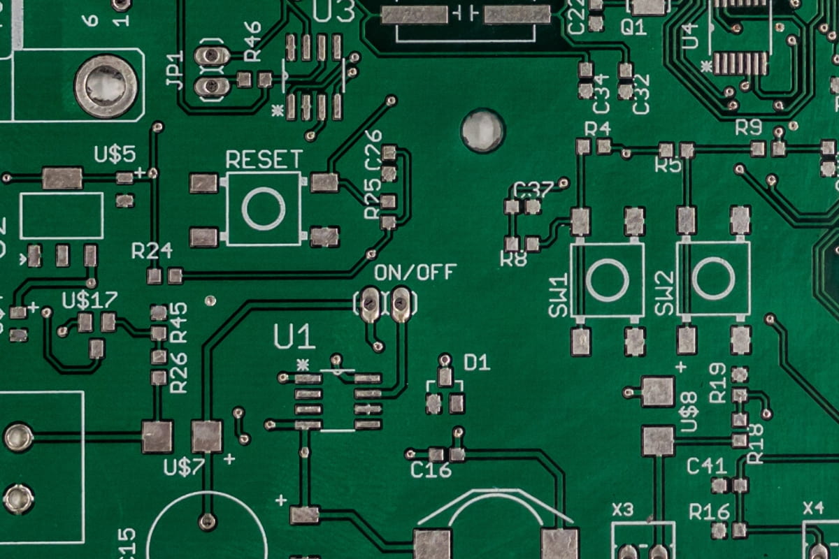
Silkscreen Printing
Silkscreen printing is the process of adding component labels, logos, and other markings to the PCB surface. This step helps with component placement and identification during assembly and troubleshooting.
Surface Finish
The final step in PCB fabrication is applying a surface finish to the exposed copper areas of the PCB. The surface finish protects the copper areas and facilitates soldering during assembly to prevent oxidation and improves the durability of the board.
Common surface finishes include HASL (Hot Air Solder Leveling), ENIG (Electroless Nickel Immersion Gold), and OSP (Organic Solderability Preservative).
Once the PCB fabrication process is complete, the finished boards undergo inspection and testing to ensure their functionality before assembly or shipping. Automated test equipment is used to identify any shorts or defects that could compromise the performance of the PCB.
How to Implement an Effective PCB Manufacturing Process
When it comes to PCB manufacturing, the design and fabrication processes are often handled by different entities. In most cases, the contract manufacturer (CM) fabricates the printed circuit board based on the design created by the original equipment manufacturer (OEM). To ensure a smooth and effective process, collaboration between these groups is essential. This collaboration includes discussions on components, design considerations, file formats, and board materials.
Components
To streamline the manufacturing process, the designer should consult with the fabricator regarding the availability of components. Ideally, the fabricator will have all the components required by the design readily available. However, if something is missing, the designer and fabricator must work together to find a compromise that allows for faster manufacturing without compromising the minimum design specifications.
Design for Manufacturing (DFM) Considerations
Design for manufacturing (DFM) is a crucial aspect to consider. DFM focuses on how well the design can progress through the various stages of the fabrication process. Typically, the fabricator, often the CM, provides a set of DFM guidelines for their facility. These guidelines can be consulted by the OEM during the design phase. By incorporating these guidelines into the PCB design, the designer can ensure that the design is compatible with the fabricator’s production process.
File Formats
Effective communication between the OEM and CM is vital to ensure the accurate fabrication of the PCB according to the OEM’s design specifications. It is essential for both parties to use the same file formats for the design. This practice helps prevent errors or lost information that may occur when files need to be converted between different formats.
Board Materials
OEMs may design printed circuit boards using more expensive materials than what the CM anticipates. Therefore, it is crucial for both parties to agree on the materials to be used. The chosen materials should not only meet the requirements of the PCB design but also remain cost-effective for the final purchaser.
By following these guidelines and fostering collaboration between the OEM and CM, an effective PCB manufacturing process can be implemented. This collaboration ensures that the design is compatible with the fabrication process, components are readily available, and the final product meets the desired specifications while remaining cost-effective.
Why Is the PCB Fabrication Process Important
PCB fabrication is important as it directly impacts the manufacturability, yield rate, reliability of printed circuit boards (PCBs) and the overall performance of the PCB. The design choices made during the fabrication process can have a significant influence on the overall performance and functionality of the PCB end product.
Manufacturability
One crucial aspect of PCB fabrication is manufacturability. Design decisions such as clearances between surface elements, selection of materials with appropriate coefficients of thermal expansion (CTE), and proper panelizing of designs are critical to ensure that the board can be built without the need for redesign.
Failing to make appropriate fabrication specification decisions during the design phase can result in issues during the manufacturing process.
Yield Rate
The yield rate of PCBs is another important factor influenced by the fabrication process. Specifying parameters that push the tolerance boundaries of the contract manufacturer’s equipment can result in a higher number of unusable boards.
By understanding the fabrication process and making informed design choices, the yield rate can be optimized, reducing waste and increasing overall efficiency.
Reliability
Reliability is also a critical consideration. Depending on the intended usage, PCBs are classified according to specific parameters outlined in IPC-6011 as it’s crucial for achieving the desired level of performance reliability. Failing to meet the necessary classification level can result in inconsistent operation or premature board failure.
Overall Performance
PCB fabrication also plays a vital role in the overall durability and efficiency of electronic devices. The fabrication process involves the selection of appropriate materials and manufacturing techniques that can withstand various environmental conditions, ensuring that the electronic device can operate reliably in different settings without experiencing premature failures or malfunctions.
Understanding the PCB fabrication process is essential because the design choices made during this stage can have a significant impact on the entire PCB development, production, and operational lifecycle. Incorporating knowledge of fabrication into design decisions can help prevent unnecessary time delays, additional manufacturing costs, and performance issues. Design for manufacturing (DFM) rules and guidelines, based on the capabilities of the contract manufacturer, can be utilized to ensure optimal results.


