
Blog
Read our blogs and insights on PCB and PCBA industry.
Blog
-
Ruggedization Services for PCBAs: Proven Protection Against Vibration and Heat
Protecting PCBAs in harsh environments requires a proven strategy. We explore the core ruggedization methods—potting, staking, and conformal coating—and explain why the choice of chemistry is the most critical decision for long-term reliability. Our approach favors simple, field-tested solutions to protect against vibration and thermal stress.
-

Life After RoHS: Navigating the End of Exemptions for Leaded BGAs
RoHS exemptions for leaded BGAs are ending, forcing hardware teams to migrate to lead-free alternatives. This is not a simple paperwork exercise but a significant reliability event, as lead-free alloys behave differently under thermal and mechanical stress, requiring a methodical plan for design, manufacturing, and validation to avoid costly field failures.
-
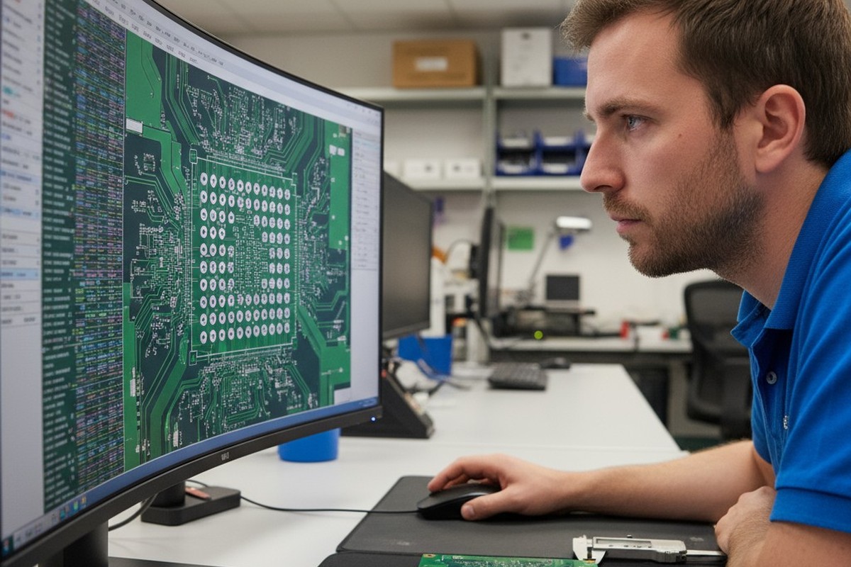
How Bester PCBA Runs Quick-Turn NPI Without Sabotaging Mass Production
Most contract manufacturers force a choice between rapid NPI and stable mass production, leading to chaos and delays. At Bester PCBA, we solve this conflict with a dedicated NPI cell architecture, early DFM checkpoints, and a golden sample lock-in protocol, creating a seamless and unbreakable bridge from prototype to high-volume manufacturing.
-

Prototype to Pilot in Thirty Days: Inside Bester PCBA’s Fast-Track Lane
Shrinking PCBA development from the standard 60-90 days to just 30 is achievable, but only with a disciplined process. This isn’t about cutting corners; it’s about optimizing three critical gates: a precise design handoff, a fixtureless testing strategy, and rapid DFM feedback. We break down the operational blueprint that dismantles structural delays and makes aggressive…
-
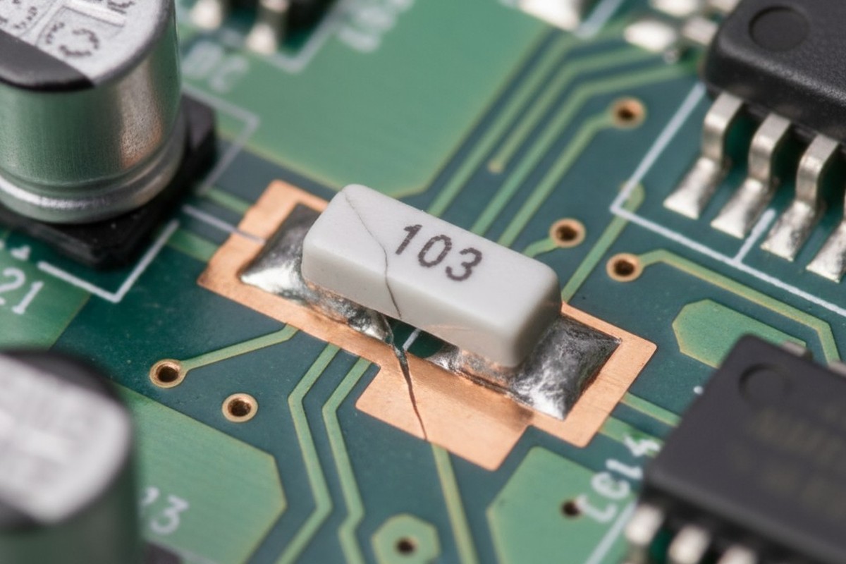
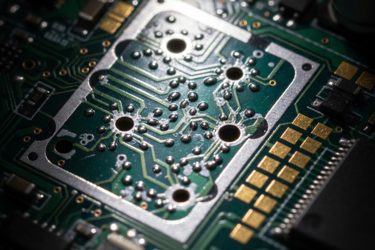
When ENIG Quietly Solves QFN Thermal Pad Voiding
Field failures from QFN thermal pad voiding are often traced back to the PCB surface finish. While HASL’s uneven topology traps flux and creates voids that degrade heat transfer, ENIG’s superior planarity ensures complete solder wetting and prevents these defects, making it a critical investment in long-term product reliability and risk mitigation.
-
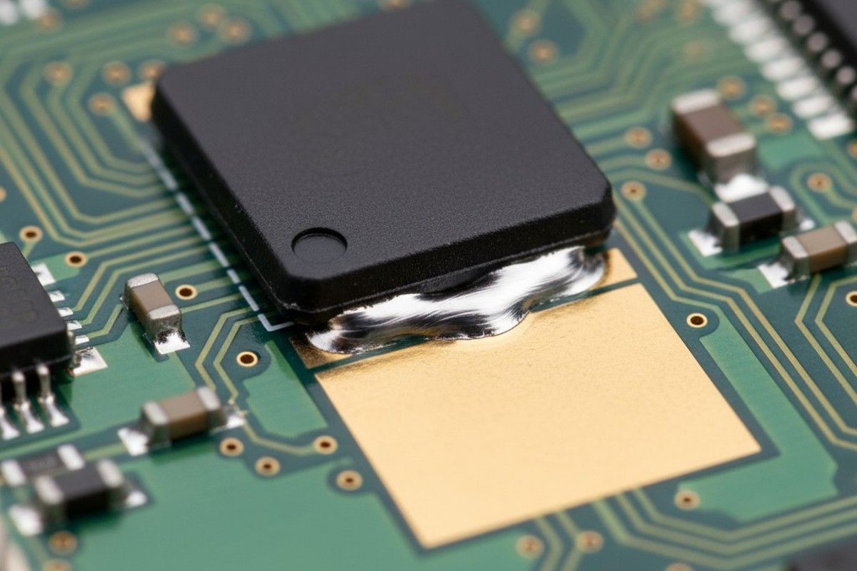
RF Shields and the Case Against Tented Vias
Tenting vias under RF shields seems like a standard practice, but it creates a semi-sealed chamber during reflow. This traps moisture and volatiles, leading to outgassing, solder ball formation, and potential short circuits. To ensure reliability, designers should avoid tenting vias under or near RF shields and instead opt for open vias to allow for…