
Blog
Read our blogs and insights on PCB and PCBA industry.
Blog
-
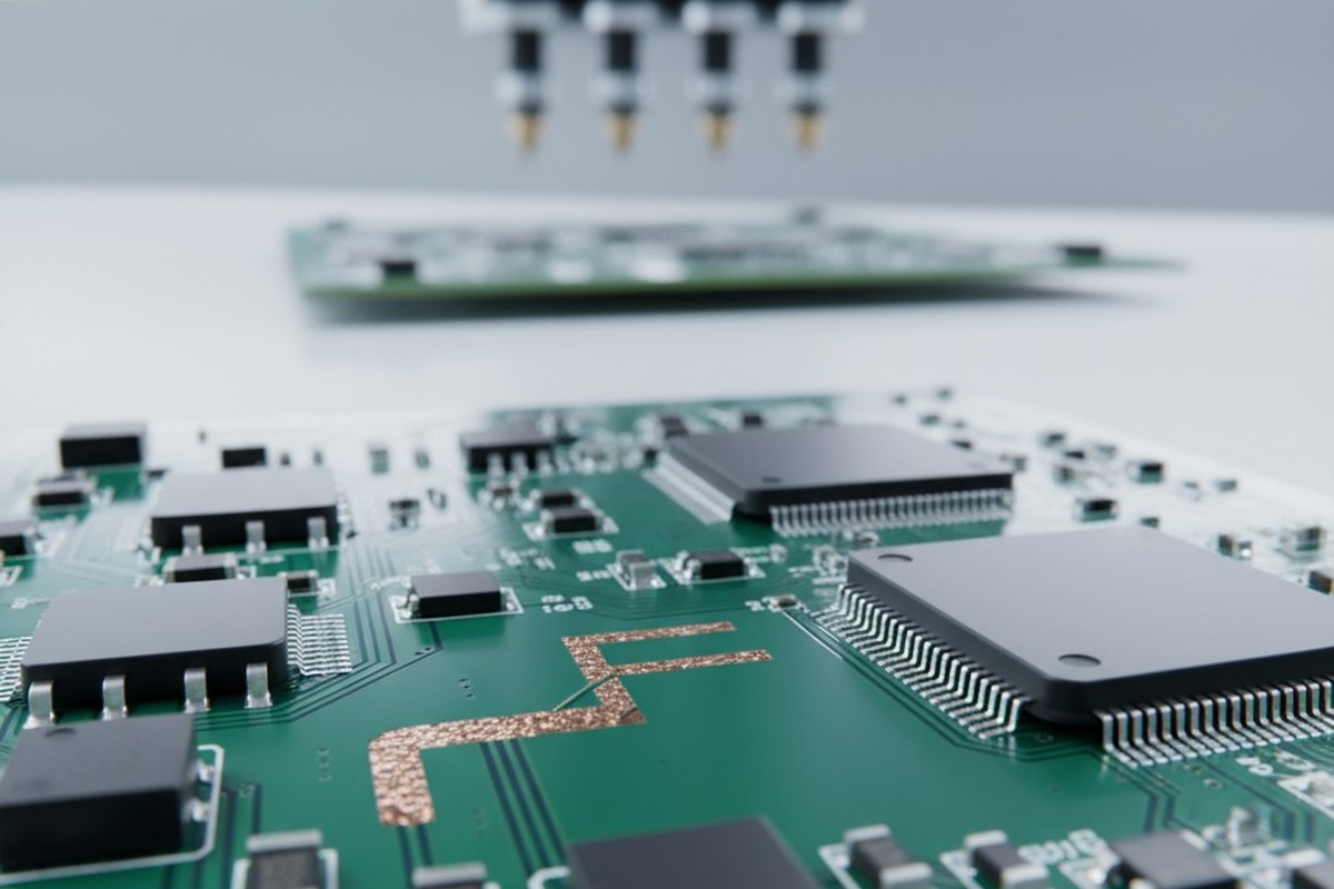
RF-Heavy IoT Boards at Bester PCBA: Assembly That Doesn’t Detune Antennas
Your IoT product’s wireless range can be compromised during manufacturing. Antenna detuning, caused by material contamination, dielectric shifts, and ground plane disruption during assembly, silently degrades RF performance. At Bester PCBA, we enforce a system of four manufacturing disciplines—from keepout zone compliance to validated test jig design—to ensure your device’s RF performance matches its design…
-
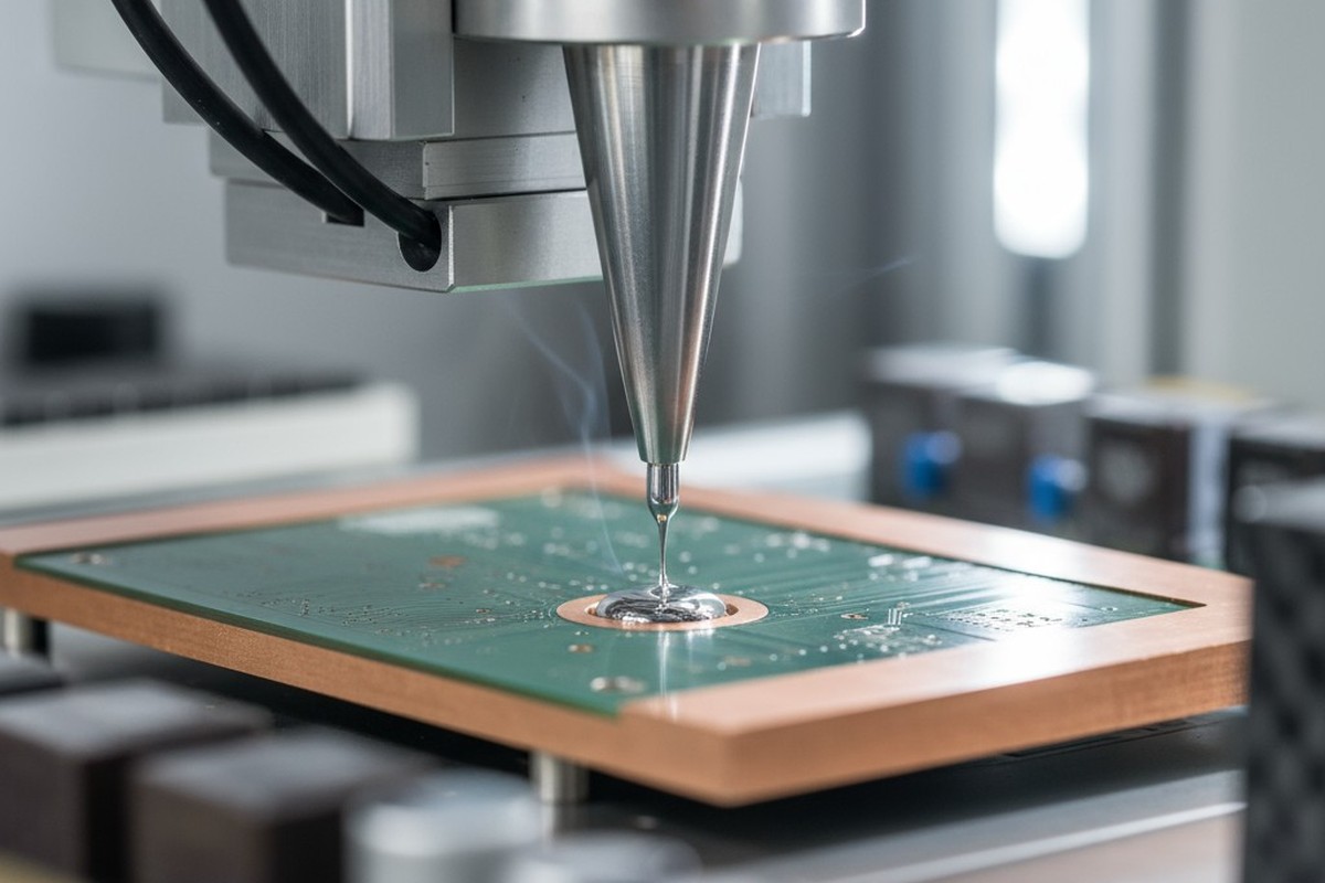
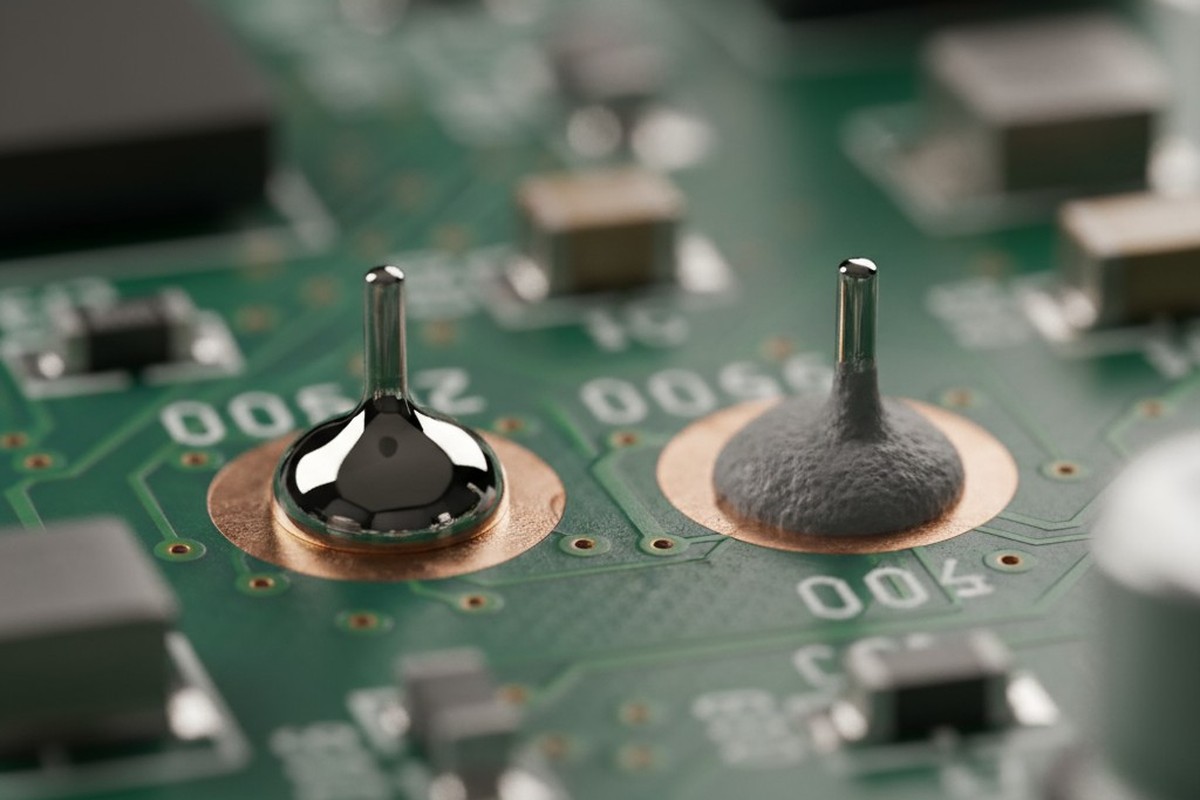
Heavy Copper and High-Current Builds at Bester PCBA That Actually Solder
Soldering heavy copper PCBs presents a significant thermal management challenge, not a skill problem. The massive thermal inertia of copper planes starves joints of heat, leading to cold joints and field failures. At Bester PCBA, we overcome this by treating it as a physics problem, using aggressive preheating and tailored process profiles to ensure robust,…
-
BOM Health Checks That Outlast Component Shortages
Component shortages often stem from preventable BOM fragilities, not unavoidable supply chain issues. By implementing systematic BOM health checks, establishing multi-source resilience through parametric qualification, and proactively monitoring component lifecycles, you can build a robust BOM that bends under supply pressure instead of breaking, ensuring production continuity.
-
Medical Device PCBA Manufacturing Under ISO 13485: Where Discipline Enables Speed
Many assume the strict regulatory discipline of ISO 13485 must slow down medical device PCBA manufacturing. This is a myth. When a quality management system is built into the core of operations, the very mechanisms that ensure traceability and repeatability, like real-time Device History Records and validated processes, become the enablers of speed and efficiency,…
-
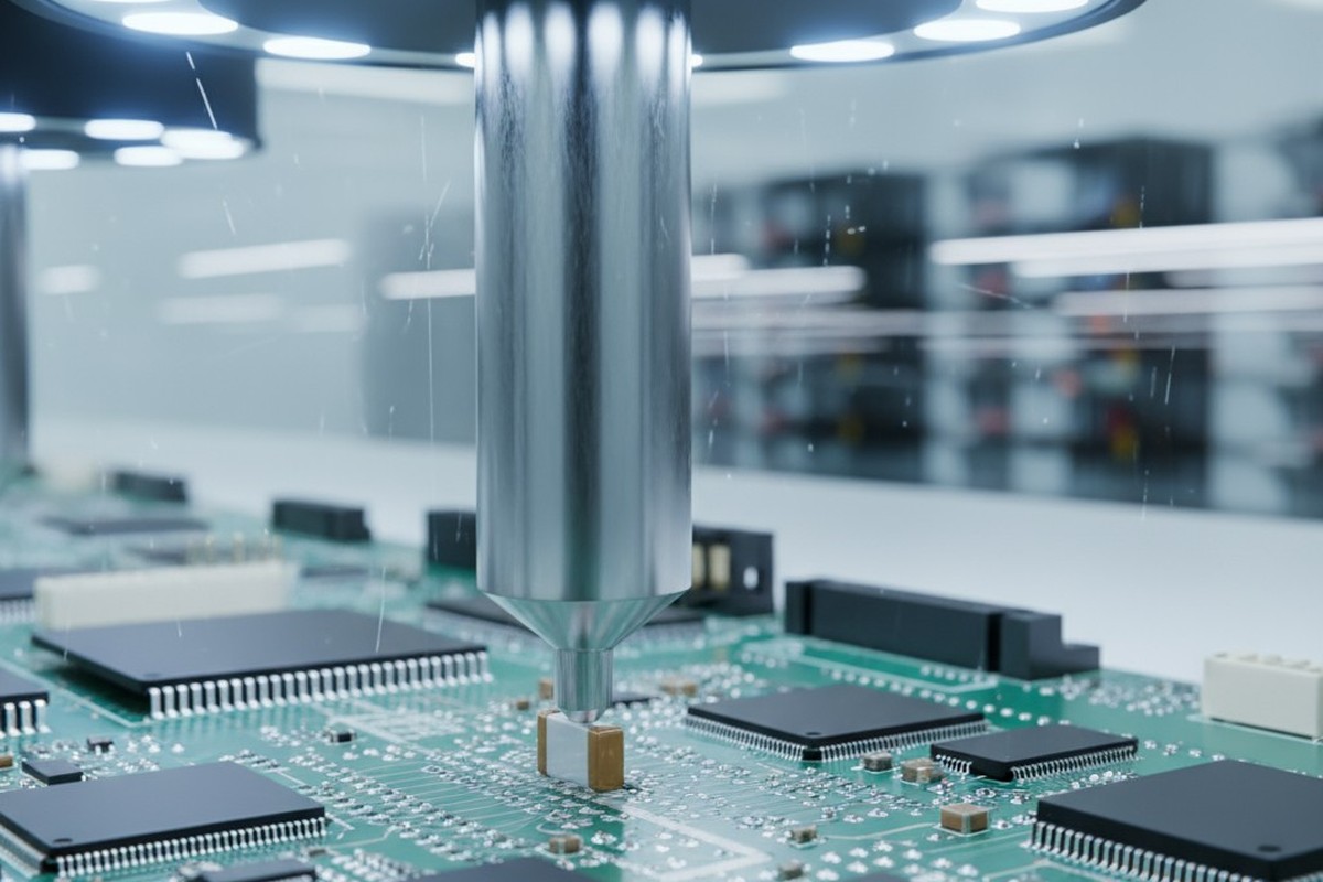
How Bester PCBA Verifies Hidden Joints: AXI Plus Power Cycling on Dense BGAs
Hidden solder joints under dense BGA packages pose a significant verification challenge. At Bester PCBA, we use a dual methodology of Automated X-ray Inspection (AXI) to assess structural quality and on-bench power cycling to validate performance under stress. This combined approach ensures both structural integrity and functional robustness, drastically reducing the risk of latent defects…
-
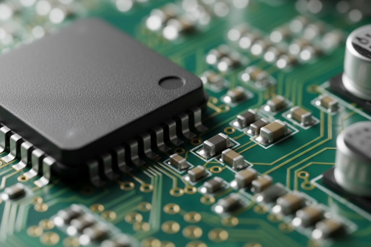
The Hidden Cost of 0402 Passives in Rugged Builds
The push for miniaturization has made 0402 passives a default choice, but this decision carries hidden costs in rugged applications. For electronics exposed to vibration and thermal stress, the slightly larger 0603 component offers superior reliability and a lower total cost of ownership by mitigating risks like tombstoning, solder joint fatigue, and costly rework.