When an LED light starts to dim prematurely, the engineering instinct is to blame the driver. Tweak the current, refine the PWM dimming, optimize the thermal foldback. These are familiar levers, and they produce measurable changes in testing. Yet the LEDs still degrade faster than predicted. The lumen maintenance curves sag. The field failures accumulate. This cycle repeats because the intervention targets a symptom, while the root cause—heat trapped at the LED junction—remains untouched.
Lumen droop is fundamentally a thermal phenomenon. An LED die’s efficiency plummets as its junction temperature rises, and no amount of electrical finesse can alter this physical reality. The heat must be removed, and its primary escape route is the mechanical assembly: the thermal stack from die to heatsink. Within this stack, two factors dominate long-term performance more than any driver setting. The first is the thermal interface material between the metal core PCB and the heatsink. The second is the manufacturing process that bonds the LED assembly to the MCPCB, specifically whether vacuum reflow is used to eliminate voids. These are not minor details to optimize later; they are the foundational decisions that determine whether a product’s thermal budget is realistic or pure fiction.
This article makes the case for why thermal interface material selection and vacuum reflow must come first. We will dissect the complete thermal stack, explain how voids sabotage heat transfer, and define realistic void limits for lighting that’s built to last.
Lumen Droop Is a Thermal Problem, Not an Electrical One
Lumen droop describes the decline in an LED’s luminous efficacy as operating conditions intensify. At the semiconductor level, this is purely about temperature. As an LED die’s junction temperature climbs, the efficiency of photon generation falls. The mechanisms involve complex physics like carrier overflow and Auger recombination, but the outcome is simple: a hotter LED produces fewer lumens per watt.
Driver circuits only influence junction temperature indirectly by controlling the power dissipated in the die. Lowering the drive current reduces power dissipation and heat, which does improve efficacy—it’s the principle behind thermal foldback algorithms. But this approach is a defensive measure, not a solution; it sacrifices light output to prevent a thermal meltdown. The fundamental challenge remains. For any target brightness, a specific amount of power must be converted in the die, and the resulting waste heat must escape. If the thermal path is blocked, the junction temperature will rise, efficiency will fall, and the driver can only choose between accepting the droop or dimming the light.
The thermal design is primary. Junction temperature dictates efficiency, reliability, and lifetime. Driver optimization is a meaningful exercise only after the thermal stack is engineered to keep that temperature in check under real-world conditions. Prioritizing electrical tweaks over thermal design is an inversion of the causal chain.
The Thermal Stack: Every Layer Between Junction and Ambient
Heat flows from the LED junction through a series of material layers and interfaces on its way to the open air. Each layer presents a thermal resistance, and these resistances add up to determine the total temperature rise. Understanding this stack reveals where design and manufacturing choices have the greatest impact.
Junction to MCPCB Base: Internal Resistances

The journey begins at the LED junction. Heat travels through the die, the die-attach material, the package base (often a ceramic or metal slug), and then the solder joint connecting the package to the metal core printed circuit board (MCPCB). Within the MCPCB, the path continues through a thin copper circuit layer, a specialized dielectric insulator, and finally into the board’s thick aluminum or copper base plate. The MCPCB’s entire purpose is to minimize resistance here, using a thin, ceramic-filled dielectric and a highly conductive metal core.
While each of these layers contributes to thermal resistance, they are largely fixed by the choice of LED and MCPCB. The designer selects components, but the internal materials and thicknesses are set by the manufacturers. The main opportunity for optimization here is in component selection, not the assembly process.
MCPCB to Heatsink: The Critical Interface
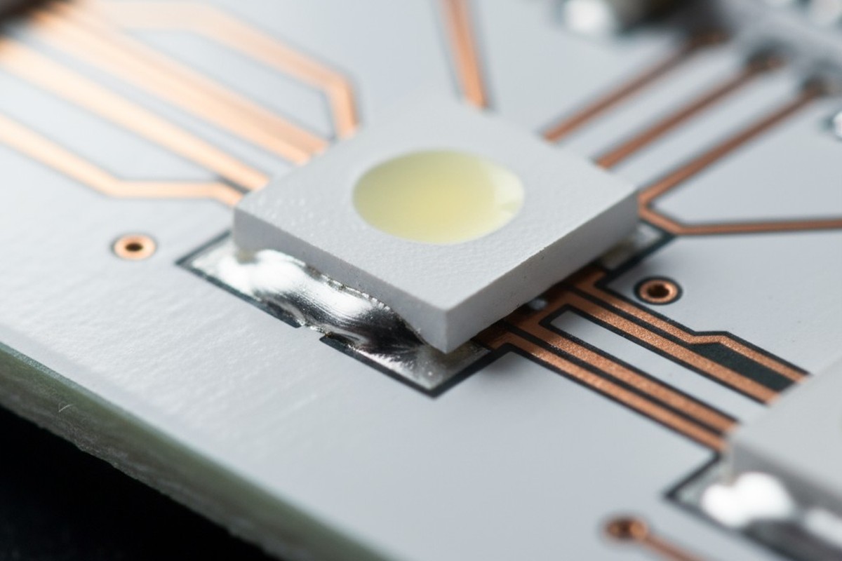
The external segment of the thermal stack, from the MCPCB base to the heatsink, is where assembly decisions have the most leverage. The MCPCB must be bonded to a heatsink to spread heat and increase the surface area for cooling. This bond relies on a thermal interface material (TIM) to fill the microscopic air gaps between the two metal surfaces. Without a TIM, these gaps would create an insulating barrier of trapped air, crippling thermal transfer.
The thermal resistance of this single interface can often exceed the sum of all internal resistances combined. This makes TIM selection the highest-leverage design choice in the entire thermal stack. A poor choice of TIM, or a sloppy application, can easily double the junction-to-ambient thermal resistance. Conversely, optimizing the TIM can unlock thermal margin that no amount of driver tuning could ever provide. The focus here is on this critical bond, where voids and material choice determine whether the heatsink’s potential is realized or wasted.
Voids: The Invisible Thermal Barrier

Voids are gas-filled gaps where a solid, conductive material was intended. In LED assemblies, they appear in two critical locations: the solder joint between the LED and the MCPCB, and the TIM layer between the MCPCB and the heatsink. In either place, they are catastrophic to thermal performance. They replace a conductive medium with trapped air, which has a thermal conductivity roughly two orders of magnitude lower than solder or a typical TIM.
A void is an invisible wall for heat.
How Voids Form During Reflow
Solder joint voids are born during the reflow process. Solder paste—a slurry of solder particles in a flux medium—is printed onto the MCPCB. During heating, the flux activates to clean metal surfaces and the solder melts, coalescing to form the bond. As the flux burns off, it releases gases. If these gases, or any trapped air, cannot escape before the solder solidifies, they become voids.
Large thermal pads, common on MCPCBs, make this problem worse. Molten solder can wet the edges of a large pad quickly, creating a seal that traps gas in the center. Atmospheric reflow processes routinely produce void percentages of 5-10% on large pads; poorly controlled processes can exceed 20%.
The Thermal Penalty of Trapped Air

The thermal conductivity of air is about 0.025 W/mK. For a typical lead-free solder, it’s closer to 50 W/mK. This two-thousand-fold difference means even a small void has a disproportionate impact. A void doesn’t just reduce the conductive area by its footprint; it disrupts the flow of heat, forcing it on a longer, more tortuous path through the surrounding solder.
Thermal models and real-world tests consistently show that the increase in thermal resistance is far greater than the void percentage suggests. A solder joint with 5% void area by X-ray can easily exhibit a 10-15% increase in thermal resistance. Voids located directly under the LED die are the most damaging. In a high-power LED assembly, this can translate directly to a 10°C rise in junction temperature, accelerating lumen depreciation and slashing the product’s effective lifetime. For any lighting product promising 50,000 hours of operation, such penalties are unacceptable.
Thermal Interface Material Selection: The Real Leverage Point
The TIM layer between the MCPCB and the heatsink is the most variable element in the thermal stack. Materials range from basic silicone greases with thermal conductivities below 1 W/mK to high-performance compounds exceeding 5 W/mK. The thickness of this layer, known as the bond line, can also vary from under 25 microns to over 100. Together, these two parameters—conductivity and thickness—determine the interface’s thermal resistance.
Beyond Thermal Conductivity
The instinct is to pick the TIM with the highest thermal conductivity. This is a mistake. The true measure is thermal resistance, calculated as bond-line thickness divided by conductivity. A high-conductivity material applied too thickly can perform worse than a lower-conductivity material applied in a thin, uniform layer.
For example, a thermal grease with a 3 W/mK conductivity applied in a 25-micron bond line is a better thermal conductor than a 5 W/mK thermal pad that is 100 microns thick. The grease wins, assuming the application process can reliably achieve that thin bond line. This is the trade-off. Greases can be messy and difficult to apply consistently, and they risk “pump-out” over time from thermal cycling. Phase-change materials offer a good compromise, applying like a solid pad but softening at operating temperatures to wet surfaces and achieve thin bond lines. Pads are the easiest to apply but their fixed thickness is a performance penalty.
Bond-Line Thickness and Application
Achieving a thin bond line depends on the TIM’s properties, the surface roughness of the parts, and the clamping pressure. Even machined aluminum surfaces are not perfectly flat. The TIM must be able to flow and fill every microscopic valley to displace air. A viscous TIM or insufficient clamping pressure will result in a thick bond line and trapped air pockets.
The application method is key. Manual application of grease is notoriously inconsistent. Automated dispensing is better but requires careful process validation. TIM selection is therefore a system-level decision, balancing material properties with manufacturing reality. The best choice is the material that delivers the lowest, most repeatable thermal resistance in your actual production environment, a conclusion that can only be reached through testing, not by reading datasheets.
Vacuum Reflow: Eliminating Voids at the Source
Vacuum reflow is a soldering process that attacks voids directly. The assembly is heated in a chamber, and once the solder is fully molten, the pressure is rapidly reduced to a near-vacuum. This simple step has a profound effect.
First, it lowers the boiling point of flux solvents, allowing them to outgas more completely. More importantly, the vacuum destabilizes any gas bubbles trapped in the molten solder. The external pressure is no longer high enough to keep them compressed. They expand, rise to the surface, and are evacuated from the joint.
The results are dramatic. Where atmospheric reflow might produce 5-10% voiding, vacuum reflow consistently achieves levels below 2%, often below 1%. This reduction in void area directly lowers thermal resistance. For high-power LED applications where every degree of thermal margin counts, vacuum reflow isn’t an incremental improvement; it’s a game-changer. While the process requires an investment in vacuum-capable ovens, the alternative is to accept higher failure rates or compensate with oversized heatsinks and lower drive currents. For any serious long-life lighting application, the economics of vacuum reflow are undeniable. The cost of a single field failure often outweighs the incremental manufacturing cost for hundreds of units.
Stencil Design for Large Thermal Pads

The stencil used to print solder paste is the first line of defense against voids. LED MCPCBs often use large thermal pads to maximize heat spreading, but standard stencil design rules don’t apply here. A single large opening in the stencil for a large pad leads to poor paste release and traps air.
The solution is to break up the single large aperture into an array of smaller ones. This improves the “area ratio”—a measure of how easily paste releases from the stencil—ensuring a clean, uniform print. The web of solder mask between these smaller apertures also creates channels for flux gases to escape during reflow. A typical design might divide a square pad into a 2×2 or 3×3 grid of smaller square or rectangular apertures, with a web of at least 0.5 mm between them.
The goal is to deposit enough solder paste for a robust joint without applying so much that it traps flux. A moderate stencil thickness of 0.10 to 0.15 mm, combined with a well-designed aperture array, usually provides the best balance. While vacuum reflow can correct for many process imperfections, it cannot rescue a disastrously poor print. Good stencil design is a prerequisite for a low-void process.
Realistic Void Limits for Long-Life Lighting
Achieving zero voids is impossible. The real question is what level of voiding is acceptable for a given application.
For standard commercial lighting with moderate power and controlled ambient temperatures, a solder joint void level below 5% is a reasonable target. This can typically be achieved with a well-controlled atmospheric reflow process. X-ray inspection should show a process mean around 2-3%, ensuring that outliers remain below the 5% ceiling.
For high-reliability applications like outdoor, automotive, or industrial lighting, the limit should be tighter. Here, below 2% is the standard. These products face higher power, higher ambient temperatures, and longer lifetime requirements, leaving no room for thermal compromise. This level of quality effectively requires vacuum reflow.
For critical systems in aerospace, medical, or safety equipment, the specification may be below 1%. Reaching this target demands stringent process controls, extended vacuum dwell times, and potentially 100% inspection, adding significant cost. This should only be specified when a risk analysis proves it necessary.
These limits shouldn’t be arbitrary. They should be established during design validation, using thermal modeling to correlate a specific void percentage to a rise in junction temperature. This data-driven approach ensures the specified limits are both necessary and sufficient—preventing thermal failures without imposing unnecessary manufacturing costs.


 Circuit Board Assembly")
