When a design file lands in the engineering queue, we don’t look at the routing or component placement first. We look at the Paste Mask layer.
Most designers treat this layer as a direct translation of the copper pads: if there is a pad on the board, there should be an aperture of the exact same size in the stencil. This 1:1 logic is neat, tidy, and mathematically perfect in a CAD environment. It’s also the single most common cause of assembly defects on modern mixed-technology boards.
The problem? A Gerber file is a two-dimensional map, but a solder joint is a three-dimensional volume. The moment we move from the screen to the manufacturing floor, we are dealing with fluid dynamics, surface tension, and the physical limitations of pushing metal paste through a steel sheet.
If we blindly cut a stencil based on the default “100% coverage” output from your ECAD software, we guarantee failure. On a board with both heavy connectors and fine-pitch microchips, a uniform approach ensures half the board has too much paste while the other half starves. We don’t modify your stencil data to be difficult; we do it because physics demands it.
Solder Is a Volume Problem
Forget “coverage.” We need to think in cubic mils.
The mechanical integrity of a joint—especially for power components and connectors—depends entirely on the volume of the resulting metallic fillet. A standard surface mount pad might look fine with a 5mil thick deposit of paste, but a through-hole reflow header or a USB-C connector is a different beast.
Designers often panic when a connector shears off during prototype testing, assuming the part itself is defective or the housing is too weak. In reality, the issue is almost always stencil thickness. A USB-C connector has structural legs that need to be anchored deep into the barrel of the PCB. If we use a standard 4mil or 5mil foil (typical for most signal boards), we deliver only a fraction of the solder required to fill that barrel. The paste prints on the surface, reflows, and disappears into the hole, leaving a weak, starved meniscus that snaps under the first insertion.
To fix this, we have to calculate the total volume of the hole minus the pin, add a 10% buffer for flux burn-off, and reverse-engineer the stencil aperture to deliver exactly that much paste. Often, the pad on the board isn’t big enough to hold that much wet paste. This forces us to overprint—intentionally printing paste on the solder mask so it pulls back onto the pad during reflow.
The Area Ratio Floor
While big parts starve, small parts have the opposite problem: they refuse to let go. This is where the “Area Ratio” rule becomes the hard floor of producibility.
Stencil printing is a battle between two forces: the surface tension of the paste sticking to the PCB pad, and the friction of the paste sticking to the inside walls of the stencil aperture. For the paste to release successfully, the area of the pad must be significantly larger than the area of the aperture walls.
The industry standard (IPC-7525) sets the danger zone at a ratio of 0.66. If the ratio drops below this (say, for a 0.4mm pitch BGA or a 01005 capacitor), the paste clogs inside the stencil rather than depositing on the board. You’ll get one good print, maybe two, and then the apertures plug up. The automated optical inspection (AOI) machine will start flagging “insufficient solder” instantly.
We can try to cheat this slightly with nano-coatings that make the steel hydrophobic, effectively greasing the walls of the aperture, but that’s a temporary patch. Those coatings wear off after 10,000 cycles or aggressive under-wipe cleaning. The only permanent engineering fix is changing the geometry: we either make the aperture larger (risking bridging) or make the stencil foil thinner to reduce the wall surface area.
The Big Part / Little Part Conflict

Now we hit the central conflict of modern electronics assembly: the “Big Part / Little Part” problem. You might have a heavy D2PAK voltage regulator that needs a mountain of solder to dissipate heat sitting right next to a 0.35mm pitch wafer-level package that needs a microscopic dusting of paste to avoid shorting out.
If we use a “standard” 5mil stencil foil—the default choice for 90% of quote requests we see—we doom one of these components. The 5mil foil provides enough volume for the D2PAK, but it’s too thick for the tiny wafer chip; the Aspect Ratio will be wrong, and the paste won’t release. If we switch to a 3mil foil to accommodate the tiny chip, the D2PAK starves, leading to voids and thermal failures.
Designers often ask, “Why can’t you just reduce the aperture size for the small part?” We can, but remember the Area Ratio: reducing the aperture area while keeping the foil thick just makes the ratio worse. You cannot solve a Z-axis problem with X-Y axis adjustments.
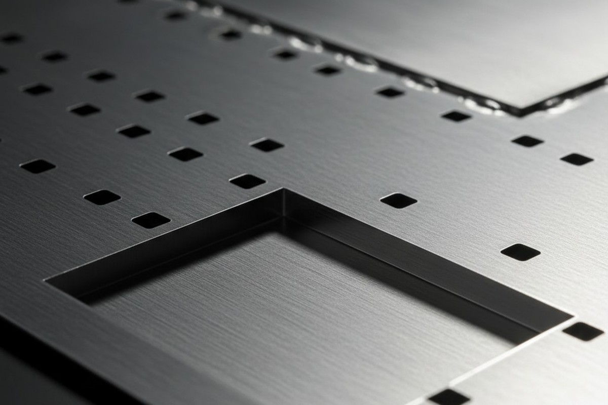
Engineering Topography: The Step Stencil

We have to treat the stencil less like a flat sheet and more like a topographic map.
We use Step Stencils to create localized thickness zones. For that D2PAK or USB connector, we might “step up” the stencil, welding a thicker tab of steel (say, 6mil or 8mil) into that specific area. For the fine-pitch BGA, we etch a “step down” pocket, reducing the thickness to 3.5mil or 3mil just for that component’s footprint.
This isn’t magic; it requires careful layout. The squeegee blade is flexible, but it’s not fluid. It needs transition space—typically 50 to 100 mils—to ride up or down the step without skipping or scooping paste out of the holes. We have to map these keep-out zones carefully, ensuring no critical components sit on the slope of the step. When done correctly, however, it allows us to print massive volumes of paste for power parts and delicate, high-definition deposits for micro-components in a single pass. It turns a board that is “unbuildable” into one that runs at 99% yield.
Window Panes and Outgassing

Geometry modifications aren’t limited to thickness. We also have to fight the behavior of the flux itself.
Under large thermal pads, like those on QFNs or power FETs, designers usually draw a solid block of paste mask matching the copper pad. If we print that, we trap a large pool of volatiles (flux vehicle) under the chip during reflow. As the flux boils, the gas has nowhere to go, creating massive voids—air bubbles inside the solder joint that block heat transfer.
To prevent this, we ignore the solid block in the Gerber and apply a “window pane” reduction. We break the large square aperture into a grid of smaller squares, separated by 10-15 mil channels of steel. These channels act as highways for the outgassing flux to escape. It sounds counter-intuitive to power engineers who want maximum thermal transfer, but printing less paste (often 60-70% coverage instead of 100%) actually results in more metal-to-metal contact because it eliminates the voiding.
The Economics of Modification
There is often pushback on the cost. A standard laser-cut stencil might cost $150 to $200. A multi-level step stencil with nano-coating might run $350 to $450. Procurement teams look at that line item and ask if we can just “make it work” with the standard option.
Compare that to the cost of the alternative.
Reworking a bridged 0.4mm BGA is not just difficult; it’s often impossible without damaging the board or neighboring components. Replacing a sheared-off connector on a finished unit costs fifty times the price of the raw part. The NRE (Non-Recurring Engineering) cost of a proper stencil is a one-time fee. The cost of scraping solder off a thousand boards because we tried to defy physics is recurring, painful, and entirely preventable. We modify the data because the cost of being right the first time is always lower than the cost of fixing it later.


 Circuit Board Assembly")


