What is External Layer
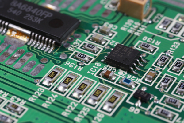
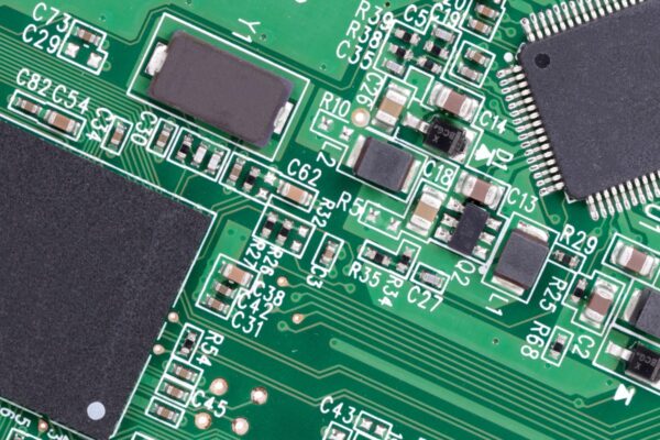
External layer is the outer copper layers or conductive patterns of a PCB. These layers are situated on the top and bottom surfaces of the PCB and serve as the primary area where electronic components are attached through soldering. The external layers begin with a copper foil, which is then subjected to an electroplating process to increase its thickness and enhance the copper content in the through-hole barrels.
The thickness of the copper foil on the external layers can be customized to meet the specific requirements of the PCB design. This customization allows for adjustments in the finished copper thickness, which in turn affects the minimum manufacturable trace widths and spacing requirements of the PCB. It is important to note that in multi-layer PCBs, the top and bottom copper layers are also referred to as the outer layers. These outer layers undergo different processing compared to the inner layers during the PCB manufacturing process.
