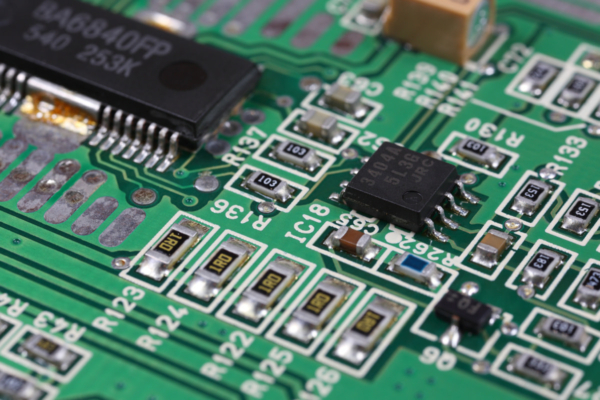
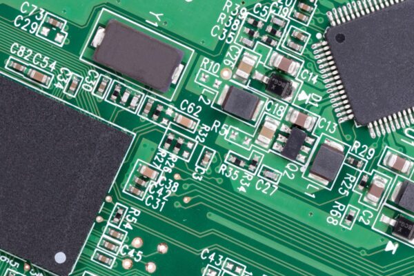
In today’s design landscape, it is up to the designer to be the master of the board layout, just as the engineer is the master of the circuitry. One of the ways a board designer can exhibit that mastery is through quality placement and routing techniques gleaned from reading and understanding the manufacturer’s data sheets and application notes.
The Changing Role of the Designer
In the past, designers used data sheets for gate and footprint information and little else, rarely reading the application notes. They relied on the engineers to explain components and/or the circuitry and to call attention to any placement or routing criticality.
But today, the role of the designer is more important due to the increasing complexity of signals, the layer structures, the changing board materials and a variety of manufacturing issues. Designers must know how the signals might react on a particular board and how to control them. They must understand how one seemingly insignificant issue might affect other design issues on the board – all items that the circuit engineer may not fully know or understand.
The Evolution of Manufacturer Information
Manufacturer information is changing just as designers’ needs are changing. Information is included today that wasn’t necessary, or wasn’t available just a few years ago. This information includes the signal rise and fall time, source and load information of the pins, impedance impedance in electricity, measure in ohms of the degree to which an electric circuit resists the flow of electric current when a voltage is impressed across its terminals, issues, placement insights, RoHS issues, assembly information, and more.
Knowing the rise and fall time of components is much more critical now because signal times are much faster, and it takes a great deal more knowledge and design effort to route signals correctly. We cannot rely on clock speed to tell us what we need to know. Attending any high-speed design class will explain why control is necessary, even on a slow clock speed board. Unfortunately, this information is not always listed in the manufacturer’s data sheets or application notes, although this would be the first place to look for it.
The Importance of Pin Assignment and Signal Routing
How can a designer place components if they don’t know what component may originate a signal? How can they route a board if they don’t know if the signal requires critical routing techniques or stub?
Stubs are used for a variety of purposes. For example, a stub might be installed in a client machine and a counterpart installed in a server, where both are required to resolve some protocol, remote procedure length control on their particular board. The pin assignment found on the data sheets should be incorporated into the library parts and defined as source or load (output or input) while also defining the function of a signal as a bus, a clock, enable, read/write, etc.
This gives access to the information needed during the layout and ECO processes. “Slow” boards are more forgiving of poor placement and routing techniques, but as all manufactured parts are getting faster, it is a good idea to design boards with these considerations in mind, even if they are irrelevant today, as any later repairs to the board will invariably use faster parts.
Impedance Specifications and Bus Length Matching
Manufacturer data sheets sometimes include impedance specifications needed for a bus or signals. This information is extremely important to signal integrity and should be followed and incorporated into board design as closely as possible. The method used to obtain that impedance is less important than that the requirement be met.
So, if the manufacturer’s information specifies a particular trace width, thickness, spacing, etc, it should be determined whether the requirements can be implemented on the board. Often, it will not, and the designer will need to calculate how to meet the impedance required using other methods.
Bus length matching information may also be included in app notes. The allowable length skew (or arrival time difference between signals) is determined by the receiving part on the bus and is typically 20 to 60 psec, which equates to about 0.100 to 0.300 inch.
So again, the information on the datasheet should be carefully considered for accuracy if it gives an arbitrarily high tolerance of +/- .050 inch. Designers should prefer information expressed in time as opposed to length because signals travel faster on outer layers of the board than inner layers.
Considerations for Placement and Routing
The placement and routing of parts based solely on information given by the manufacturer causes some controversy but is still worthy of consideration. While the information may not take into account all the specific issues on a particular board, the designer should read and understand the manufacturer’s technical data to understand the requirements of the part. If the information does not seem valid for a particular design, a discussion with the circuit designer, manufacturing, or test and repair people may be in order.
Incorporating New Manufacturing Issues
The designer must also incorporate new manufacturing issues, including RoHS compliance information, into the parts and board layout. These issues may include, but not limited to, solder mask type or size required, solder paste type or stencil thickness, squeegee pressure, paste opening size and shape, step-stencil specifications, cleaning information, thermal cycles, and wave and reflow soldering information.
Conclusion
Designers must read and learn to incorporate technical data and accompanying design requirements to become the board layout masters needed today. Whether a new design is complex, wide open, or slow or fast, the signal integrity and EMI (RFI) from chips and other electronic devices. Allowable limits are governed by the FCC. (and thus board performance) can be affected by how components are placed and traces routed. It is vitally important that the designer understands the information provided by the manufacturer and incorporates any applicable data into their board layout.


